JAJSHP1E July 2014 – June 2022 ADC3221 , ADC3222 , ADC3223 , ADC3224
PRODUCTION DATA
- 1 特長
- 2 アプリケーション
- 3 概要
- 4 Revision History
- 5 Pin Configuration and Functions
-
6 Specifications
- 6.1 Absolute Maximum Ratings
- 6.2 ESD Ratings
- 6.3 Recommended Operating Conditions (1)
- 6.4 Thermal Information
- 6.5 Electrical Characteristics: General
- 6.6 Electrical Characteristics: ADC3221, ADC3222
- 6.7 Electrical Characteristics: ADC3223, ADC3224
- 6.8 AC Performance: ADC3221
- 6.9 AC Performance: ADC3222
- 6.10 AC Performance: ADC3223
- 6.11 AC Performance: ADC3224
- 6.12 Digital Characteristics
- 6.13 Timing Requirements: General
- 6.14 Timing Requirements: LVDS Output
- 6.15 Typical Characteristics: ADC3221
- 6.16 Typical Characteristics: ADC3222
- 6.17 Typical Characteristics: ADC3223
- 6.18 Typical Characteristics: ADC3224
- 6.19 Typical Characteristics: Common
- 6.20 Typical Characteristics: Contour
- 7 Parameter Measurement Information
-
8 Detailed Description
- 8.1 Overview
- 8.2 Functional Block Diagram
- 8.3 Feature Description
- 8.4 Device Functional Modes
- 8.5 Programming
- 8.6
Register Maps
- 8.6.1 Summary of Special Mode Registers
- 8.6.2
Serial Register Description
- 8.6.2.1 Register 01h
- 8.6.2.2 Register 03h
- 8.6.2.3 Register 04h
- 8.6.2.4 Register 05h
- 8.6.2.5 Register 06h
- 8.6.2.6 Register 07h
- 8.6.2.7 Register 09h
- 8.6.2.8 Register 0Ah
- 8.6.2.9 Register 0Bh
- 8.6.2.10 Register 0Eh
- 8.6.2.11 Register 0Fh
- 8.6.2.12 Register 13h
- 8.6.2.13 Register 15h
- 8.6.2.14 Register 25h
- 8.6.2.15 Register 27h
- 8.6.2.16 Register 41Dh
- 8.6.2.17 Register 422h
- 8.6.2.18 Register 434h
- 8.6.2.19 Register 439h
- 8.6.2.20 Register 51Dh
- 8.6.2.21 Register 522h
- 8.6.2.22 Register 534h
- 8.6.2.23 Register 539h
- 8.6.2.24 Register 608h
- 8.6.2.25 Register 70Ah
- 9 Applications and Implementation
- 10Device and Documentation Support
- 11Mechanical, Packaging, and Orderable Information
パッケージ・オプション
メカニカル・データ(パッケージ|ピン)
- RGZ|48
サーマルパッド・メカニカル・データ
- RGZ|48
発注情報
8.3.2 Clock Input
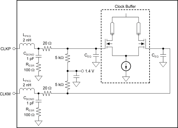
The device clock inputs can be driven differentially (sine, LVPECL, or LVDS) or single-ended (LVCMOS), with little or no difference in performance between them. The common-mode voltage of the clock inputs is set to
0.95 V using internal 5-kΩ resistors. The self-bias clock inputs of the ADC322x can be driven by the transformer-coupled, sine-wave clock source or by the ac-coupled, LVPECL and LVDS clock sources, as shown in Figure 8-1, Figure 8-2, and Figure 8-3. See Figure 8-4 for details regarding the internal clock buffer.
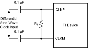
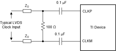 Figure 8-2 LVDS Clock Driving Circuit
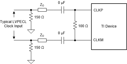 Figure 8-3 LVPECL Clock Driving Circuit
A single-ended CMOS clock can be ac-coupled to the CLKP input, with CLKM connected to ground with a 0.1-μF capacitor, as shown in Figure 8-5. However, for best performance the clock inputs must be driven differentially, thereby reducing susceptibility to common-mode noise. For high input frequency sampling, TI recommends using a clock source with very low jitter. Band-pass filtering of the clock source can help reduce the effects of jitter. There is no change in performance with a non-50% duty cycle clock input.
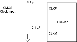 Figure 8-5 Single-Ended Clock Driving Circuit