JAJSQJ8 January   2024 ADS1014L , ADS1015L

PRODUCTION DATA  

  1.   1
  2. 特長
  3. アプリケーション
  4. 概要
  5. Device Comparison Table
  6. Pin Configuration and Functions
  7. Specifications
    1. 6.1 Absolute Maximum Ratings
    2. 6.2 ESD Ratings
    3. 6.3 Recommended Operating Conditions
    4. 6.4 Thermal Information
    5. 6.5 Electrical Characteristics
    6. 6.6 I2C Timing Requirements
    7. 6.7 Timing Diagram
  8. Detailed Description
    1. 7.1 Overview
    2. 7.2 Functional Block Diagrams
    3. 7.3 Feature Description
      1. 7.3.1 Multiplexer
      2. 7.3.2 Analog Inputs
      3. 7.3.3 Full-Scale Range (FSR) and LSB Size
      4. 7.3.4 Voltage Reference
      5. 7.3.5 Oscillator
      6. 7.3.6 Output Data Rate and Conversion Time
      7. 7.3.7 Digital Comparator
      8. 7.3.8 Conversion-Ready Pin
      9. 7.3.9 SMBus Alert Response
    4. 7.4 Device Functional Modes
      1. 7.4.1 Reset and Power-Up
      2. 7.4.2 Operating Modes
        1. 7.4.2.1 Single-Shot Mode
        2. 7.4.2.2 Continuous-Conversion Mode
    5. 7.5 Programming
      1. 7.5.1 I2C Interface
        1. 7.5.1.1 I2C Address Selection
        2. 7.5.1.2 I2C Interface Speed
          1. 7.5.1.2.1 Serial Clock (SCL) and Serial Data (SDA)
        3. 7.5.1.3 I2C Data Transfer Protocol
        4. 7.5.1.4 Timeout
        5. 7.5.1.5 I2C General-Call (Software Reset)
      2. 7.5.2 Reading and Writing Register Data
        1. 7.5.2.1 Reading Conversion Data or the Configuration Register
        2. 7.5.2.2 Writing the Configuration Register
      3. 7.5.3 Data Format
  9. Register Map
  10. Application and Implementation
    1. 9.1 Application Information
      1. 9.1.1 Basic Connections
      2. 9.1.2 Unused Inputs and Outputs
      3. 9.1.3 Single-Ended Inputs
      4. 9.1.4 Input Protection
      5. 9.1.5 Analog Input Filtering
      6. 9.1.6 Connecting Multiple Devices
      7. 9.1.7 Duty Cycling For Low Power
      8. 9.1.8 I2C Communication Sequence Example
    2. 9.2 Typical Application
      1. 9.2.1 Design Requirements
      2. 9.2.2 Detailed Design Procedure
      3. 9.2.3 Application Curve
    3. 9.3 Power Supply Recommendations
      1. 9.3.1 Power-Supply Sequencing
      2. 9.3.2 Power-Supply Decoupling
    4. 9.4 Layout
      1. 9.4.1 Layout Guidelines
      2. 9.4.2 Layout Example
  11. 10Device and Documentation Support
    1. 10.1 ドキュメントの更新通知を受け取る方法
    2. 10.2 サポート・リソース
    3. 10.3 Trademarks
    4. 10.4 静電気放電に関する注意事項
    5. 10.5 用語集
  12. 11Revision History
  13. 12Mechanical, Packaging, and Orderable Information

パッケージ・オプション

メカニカル・データ(パッケージ|ピン)
サーマルパッド・メカニカル・データ
発注情報

Digital Comparator

The ADS101xL features a programmable digital comparator that can issue an alert on the ALERT/RDY pin. The COMP_MODE bit in the Configuration register configures the comparator as either a traditional comparator or a window comparator. In traditional comparator mode, the ALERT/RDY pin asserts (active low by default) when conversion data exceed the limit set in the High-threshold register (Hi_thresh). The comparator then deasserts only when the conversion data falls below the limit set in the Low-threshold register (Lo_thresh). In window comparator mode, the ALERT/RDY pin asserts when the conversion data exceed the Hi_thresh register or fall below the Lo_thresh register value.

In either window or traditional comparator mode, the comparator can be configured to latch after being asserted by the COMP_LAT bit in the Configuration register. This setting causes the assertion to remain even if the input signal is not beyond the bounds of the threshold registers. This latched assertion can only be cleared by issuing an SMBus alert response or by reading the Conversion register. The ALERT/RDY pin can be configured as active high or active low by the COMP_POL bit in the Configuration register. Figure 7-6 shows operational diagrams for both comparator modes.

The comparator can also be configured to activate the ALERT/RDY pin only after a set number of successive readings exceed the threshold values set in the threshold registers (Hi_thresh and Lo_thresh). The COMP_QUE[1:0] bits in the Configuration register configure the comparator to wait for one, two, or four readings beyond the threshold before activating the ALERT/RDY pin. The COMP_QUE[1:0] bits can also disable the comparator function and put the ALERT/RDY pin into a high state.
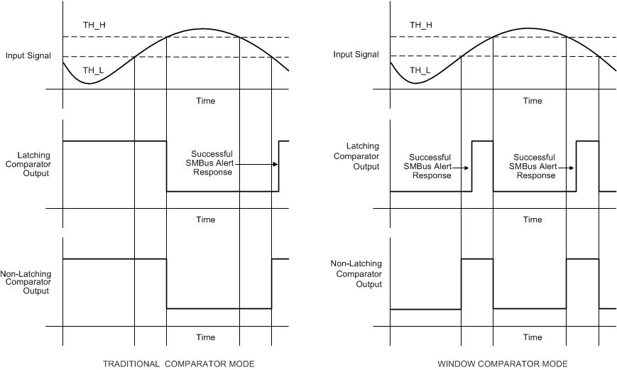
GUID-3840D462-85B3-4913-95E8-9BD93091E533-low.gifFigure 7-6 ALERT Pin Timing Diagram