JAJS456G July 2009 – August 2016 ADS1146 , ADS1147 , ADS1148
PRODUCTION DATA.
- 1 特長
- 2 アプリケーション
- 3 概要
- 4 改訂履歴
- 5 Device Comparison Table
- 6 Pin Configuration and Functions
- 7 Specifications
- 8 Parameter Measurement Information
-
9 Detailed Description
- 9.1 Overview
- 9.2 Functional Block Diagrams
- 9.3
Feature Description
- 9.3.1 ADC Input and Multiplexer
- 9.3.2 Low-Noise PGA
- 9.3.3 Clock Source
- 9.3.4 Modulator
- 9.3.5 Digital Filter
- 9.3.6 Voltage Reference Input
- 9.3.7 Internal Voltage Reference
- 9.3.8 Excitation Current Sources
- 9.3.9 Sensor Detection
- 9.3.10 Bias Voltage Generation
- 9.3.11 General-Purpose Digital I/O
- 9.3.12 System Monitor
- 9.4 Device Functional Modes
- 9.5
Programming
- 9.5.1 Digital Interface
- 9.5.2 Data Format
- 9.5.3
Commands
- 9.5.3.1 WAKEUP (0000 000x)
- 9.5.3.2 SLEEP (0000 001x)
- 9.5.3.3 SYNC (0000 010x)
- 9.5.3.4 RESET (0000 011x)
- 9.5.3.5 RDATA (0001 001x)
- 9.5.3.6 RDATAC (0001 010x)
- 9.5.3.7 SDATAC (0001 011x)
- 9.5.3.8 RREG (0010 rrrr, 0000 nnnn)
- 9.5.3.9 WREG (0100 rrrr, 0000 nnnn)
- 9.5.3.10 SYSOCAL (0110 0000)
- 9.5.3.11 SYSGCAL (0110 0001)
- 9.5.3.12 SELFOCAL (0110 0010)
- 9.5.3.13 NOP (1111 1111)
- 9.5.3.14 Restricted Command (1111 0001)
- 9.6
Register Maps
- 9.6.1 ADS1146 Register Map
- 9.6.2
ADS1146 Detailed Register Definitions
- 9.6.2.1 BCS—Burn-out Current Source Register (offset = 00h) [reset = 01h]
- 9.6.2.2 VBIAS—Bias Voltage Register (offset = 01h) [reset = 00h]
- 9.6.2.3 MUX—Multiplexer Control Register (offset = 02h) [reset = x0h]
- 9.6.2.4 SYS0—System Control Register 0 (offset = 03h) [reset = 00h]
- 9.6.2.5 OFC—Offset Calibration Coefficient Registers (offset = 04h, 05h, 06h) [reset = 00h, 00h, 00h]
- 9.6.2.6 FSC—Full-Scale Calibration Coefficient Registers (offset = 07h, 08h, 09h) [reset = 00h, 00h, 40h]
- 9.6.2.7 ID—ID Register (offset = 0Ah) [reset = x0h]
- 9.6.3 ADS1147 and ADS1148 Register Map
- 9.6.4
ADS1147 and ADS1148 Detailed Register Definitions
- 9.6.4.1 MUX0—Multiplexer Control Register 0 (offset = 00h) [reset = 01h]
- 9.6.4.2 VBIAS—Bias Voltage Register (offset = 01h) [reset = 00h]
- 9.6.4.3 MUX1—Multiplexer Control Register 1 (offset = 02h) [reset = x0h]
- 9.6.4.4 SYS0—System Control Register 0 (offset = 03h) [reset = 00h]
- 9.6.4.5 OFC—Offset Calibration Coefficient Register (offset = 04h, 05h, 06h) [reset = 00h, 00h, 00h]
- 9.6.4.6 FSC—Full-Scale Calibration Coefficient Register (offset = 07h, 08h, 09h) [reset = 00h, 00h, 40h]
- 9.6.4.7 IDAC0—IDAC Control Register 0 (offset = 0Ah) [reset = x0h]
- 9.6.4.8 IDAC1—IDAC Control Register 1 (offset = 0Bh) [reset = FFh]
- 9.6.4.9 GPIOCFG—GPIO Configuration Register (offset = 0Ch) [reset = 00h]
- 9.6.4.10 GPIODIR—GPIO Direction Register (offset = 0Dh) [reset = 00h]
- 9.6.4.11 GPIODAT—GPIO Data Register (offset = 0Eh) [reset = 00h]
-
10Application and Implementation
- 10.1
Application Information
- 10.1.1 Serial Interface Connections
- 10.1.2 Analog Input Filtering
- 10.1.3 External Reference and Ratiometric Measurements
- 10.1.4 Establishing a Proper Common-Mode Input Voltage
- 10.1.5 Isolated (or Floating) Sensor Inputs
- 10.1.6 Unused Inputs and Outputs
- 10.1.7 Pseudo Code Example
- 10.1.8 Channel Multiplexing Example
- 10.1.9 Power-Down Mode Example
- 10.2 Typical Applications
- 10.3 Do's and Don'ts
- 10.1
Application Information
- 11Power Supply Recommendations
- 12Layout
- 13デバイスおよびドキュメントのサポート
- 14メカニカル、パッケージ、および注文情報
パッケージ・オプション
メカニカル・データ(パッケージ|ピン)
サーマルパッド・メカニカル・データ
- RHB|32
発注情報
10 Application and Implementation
NOTE
Information in the following applications sections is not part of the TI component specification, and TI does not warrant its accuracy or completeness. TI’s customers are responsible for determining suitability of components for their purposes. Customers should validate and test their design implementation to confirm system functionality.
10.1 Application Information
The ADS1146, ADS1147, and ADS1148 make up a family of precision, 16-bit, ΔΣ ADCs that offers many integrated features to ease the measurement of the most common sensor types including various types of temperature and bridge sensors. Primary considerations when designing an application with these devices include connecting and configuring the serial interface, designing the analog input filtering, establishing an appropriate external reference for ratiometric measurements, and setting the common-mode input voltage for the internal PGA. These considerations are discussed in the following sections.
10.1.1 Serial Interface Connections
Figure 77 shows the principle serial interface connections for the ADS1148.
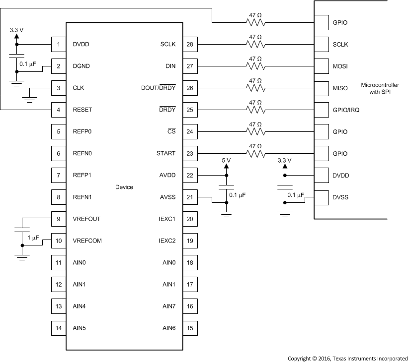 Figure 77. Serial Interface Connections
Most microcontroller SPI peripherals can operate with the ADS1148. The interface operates in SPI mode 1 where CPOL = 0 and CPHA = 1. In SPI mode 1, SCLK idles low and data are launched or changed only on SCLK rising edges; data are latched or read by the master and slave on SCLK falling edges. Details of the SPI communication protocol employed by the device can be found in the Serial Interface Timing Requirements section.
TI recommends placing 47-Ω resistors in series with all digital input and output pins (CS, SCLK, DIN, DOUT/DRDY, DRDY, RESET and START). This resistance smooths sharp transitions, suppresses overshoot, and offers some overvoltage protection. Care must be taken to meet all SPI timing requirements because the additional resistors interact with the bus capacitances present on the digital signal lines.
10.1.2 Analog Input Filtering
Analog input filtering serves two purposes: first, to limit the effect of aliasing during the sampling process and second, to reduce external noise from being a part of the measurement.
As with any sampled system, aliasing can occur if proper anti-alias filtering is not in place. Aliasing occurs when frequency components are present in the input signal that are higher than half the sampling frequency of the ADC (also known as the Nyquist frequency). These frequency components are folded back and show up in the actual frequency band of interest below half the sampling frequency. Note that inside a ΔΣ ADC, the input signal is sampled at the modulator frequency, fMOD and not at the output data rate. The filter response of the digital filter repeats at multiples of the fMOD, as shown in Figure 78. Signals or noise up to a frequency where the filter response repeats are attenuated to a certain amount by the digital filter depending on the filter architecture. Any frequency components present in the input signal around the modulator frequency or multiples thereof are not attenuated and alias back into the band of interest, unless attenuated by an external analog filter.
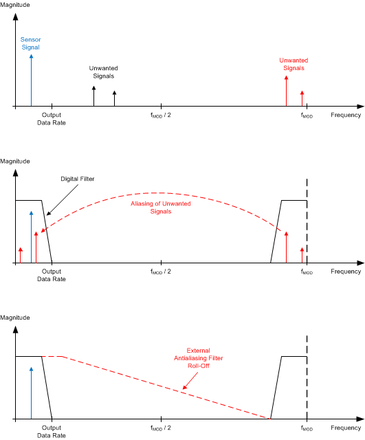 Figure 78. Effect of Aliasing
Many sensor signals are inherently bandlimited; for example, the output of a thermocouple has a limited rate of change. In this case, the sensor signal does not alias back into the pass-band when using a ΔΣ ADC. However, any noise pickup along the sensor wiring or the application circuitry can potentially alias into the pass-band. Power line-cycle frequency and harmonics are one common noise source. External noise can also be generated from electromagnetic interference (EMI) or radio frequency interference (RFI) sources, such as nearby motors and cellular phones. Another noise source typically exists on the printed-circuit board (PCB) itself in the form of clocks and other digital signals. Analog input filtering helps remove unwanted signals from affecting the measurement result.
A first-order resistor-capacitor (RC) filter is (in most cases) sufficient to either totally eliminate aliasing, or to reduce the effect of aliasing to a level within the noise floor of the sensor. Ideally, any signal beyond fMOD/2 is attenuated to a level below the noise floor of the ADC. The digital filter of the ADS1148 attenuates signals to a certain degree, as illustrated in the filter response plots in the Digital Filter section. In addition, noise components are usually smaller in magnitude than the actual sensor signal. Therefore, using a first-order RC filter with a cutoff frequency set at the output data rate or 10× higher is generally a good starting point for a system design.
Internal to the device, prior to the PGA inputs, is an EMI filter; see Figure 20. The cutoff frequency of this filter is approximately 47 MHz, which helps reject high-frequency interferences.
10.1.3 External Reference and Ratiometric Measurements
The full-scale range of the ADS1148 is defined by the reference voltage and the PGA gain (FSR = ±VREF / Gain). An external reference can be used instead of the integrated 2.048-V reference to adapt the FSR to the specific system requirements. An external reference must be used if VIN > 2.048 V. For example, an external 2.5-V reference is required to measure signals as large as 2.5 V. Note that the input signal must be within the common-mode input range to be valid, and that the reference input voltage must be between 0.5 V and
(AVDD – AVSS – 1 V).
The buffered reference inputs of the device also allow the implementation of ratiometric measurements. In a ratiometric measurement, the same excitation source that is used to excite the sensor is also used to establish the reference for the ADC. As an example, a simple form of a ratiometric measurement uses the same current source to excite both the resistive sensor element (such as an RTD) and another resistive reference element that is in series with the element being measured. The voltage that develops across the reference element is used as the reference source for the ADC. In this configuration, current noise and drift are common to both the sensor measurement and the reference; therefore, these components cancel out in the ADC transfer function. The output code is only a ratio of the sensor element value and the reference resistor value, and is not affected by the absolute value of the excitation current.
10.1.4 Establishing a Proper Common-Mode Input Voltage
The ADS1148 is used to measure various types of signal configurations. However, configuring the input of the device properly for the respective signal type is important.
The ADS1148 features an 8-input multiplexer (while the ADS1147 has a 4-input multiplexer). Each input can be independently selected as the positive input or the negative input to be measured by the ADC. With an 8-input multiplexer, the user can measure four independent differential-input channels. The user can also choose to measure 7 channels, using one input as a fixed common input. Regardless of the analog input configuration, make sure that all inputs, including the common input are within the common-mode input voltage range.
If the supply is unipolar (for example, AVSS = 0 V and AVDD = 5 V), then V(AINN) = 0 V is not within the common-mode input range as shown by Equation 3. Therefore, a single-ended measurement with the common input connected to ground is not possible. TI recommends connecting the common-input to mid-supply or alternatively to VREFOUT. Note that the common-mode range becomes further restricted with increasing PGA gain.
If the supply is bipolar (AVSS = –2.5 V and AVDD = 2.5 V), then ground is within the common-mode input range. Single-ended measurements with the common input connected to 0 V are possible in this case.
For a detailed explanation of the common-mode input range as it relates to the PGA see the PGA Common-Mode Voltage Requirements section.
10.1.5 Isolated (or Floating) Sensor Inputs
Isolated sensors (sensors that are not referenced to the ADC ground) must have a common-mode voltage established within the specified ADC input range. Level shift the common-mode voltage by external resistor biasing, by connecting the negative lead to ground (bipolar analog supply), or by connecting to a DC voltage (unipolar analog supply). The 2.048-V reference output voltage may also be used to provide level shifting to floating sensor inputs.
10.1.6 Unused Inputs and Outputs
To minimize leakage currents on the analog inputs, leave unused analog inputs floating, connect them to mid-supply, or connect them to AVDD. Connecting unused analog inputs to AVSS is possible as well, but can yield higher leakage currents than the options mentioned before.
Do not float unused digital inputs or excessive power-supply leakage current may result. Tie all unused digital inputs to the appropriate levels, DVDD or DGND, including when in power-down mode. If the DRDY output is not used, leave the pin unconnected or tie it to DVDD using a weak pullup resistor.
10.1.7 Pseudo Code Example
The following list shows a pseudo code sequence with the required steps to set up the device and the microcontroller that interfaces to the ADC to take subsequent readings from the ADS1148 in stop read data continuous (SDATAC) mode. In SDATAC mode, it is sufficient to wait for a time period longer than the data rate to retrieve the conversion result. New conversion data does not interrupt the reading of registers or data on DOUT. However in this example, the dedicated DRDY pin is used to indicate availability of new conversion data instead of waiting a set time period for a readout. The default configuration register settings are changed to PGA gain = 16, using the internal reference, and a data rate of 20 SPS.
Power up;
Delay for a minimum of 16 ms to allow power supplies to settle and power-on reset to complete;
Enable the device by setting the START pin high;
Configure the serial interface of the microcontroller to SPI mode 1 (CPOL = 0, CPHA =1);
If the CS pin is not tied low permanently, configure the microcontroller GPIO connected to CS as an output;
Configure the microcontroller GPIO connected to the DRDY pin as a falling edge triggered interrupt input;
Set CS to the device low;
Delay for a minimum of tCSSC;
Send the RESET command (06h) to make sure the device is properly reset after power up;
Delay for a minimum of 0.6 ms;
Send SDATAC command (16h) to prevent the new data from interrupting data or register transactions;
Write the respective register configuration with the WREG command (40h, 03h, 01h, 00h, 03h and 42h);
As an optional sanity check, read back all configuration registers with the RREG command (four bytes from 20h, 03h);
Send the SYNC command (04h) to start the ADC conversion;
Delay for a minimum of tSCCS;
Clear CS to high (resets the serial interface);
Loop
{
	Wait for DRDY to transition low;
	Take CS low;
	Delay for a minimum of tCSSC;
	Send the RDATA command (12h);
	Send 16 SCLKs to read out conversion data on DOUT/DRDY;
	Delay for a minimum of tSCCS;
	Clear CS to high;
}
Take CS low;
Delay for a minimum of tCSSC;
Send the SLEEP command (02h) to stop conversions and put the device in power-down mode;
10.1.8 Channel Multiplexing Example
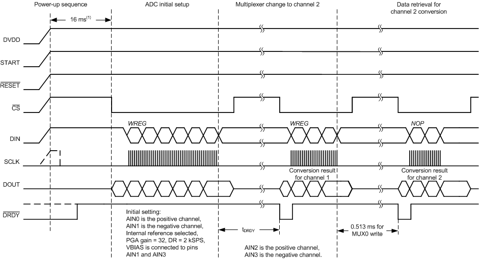
This example applies only to the ADS1147 and ADS1148. It explains a method to use the device with two sensors connected to two different analog channels. Figure 79 shows the sequence of SPI operations performed on the device. After power up, 216 tCLK cycles are required before communication can be started. During the first 216 tCLK cycles, the device is internally held in a reset state. In this example, one of the sensors is connected to channels AIN0 and AIN1 and the other sensor is connected to channels AIN2 and AIN3. The ADC is operated at a data rate of 2 kSPS. The PGA gain is set to 32 for both sensors. VBIAS is connected to the negative terminal of both sensors (that is, channels AIN1 and AIN3). All these settings can be changed by performing a block write operation on the first four registers of the device. After the DRDY pin goes low, the conversion result can be immediately retrieved by sending in 16 SCLK pulses because the device defaults to RDATAC mode. As the conversion result is being retrieved, the active input channels can be switched to AIN2 and AIN3 by writing into the MUX0 register in a full-duplex manner, as shown in Figure 79. The write operation is completed with an additional eight SCLK pulses. The time from the write operation into the MUX0 register to the next DRDY low transition is shown in Figure 79 and is 0.513 ms in this case. After DRDY goes low, the conversion result can be retrieved and the active channel can be switched as before.
10.1.9 Power-Down Mode Example
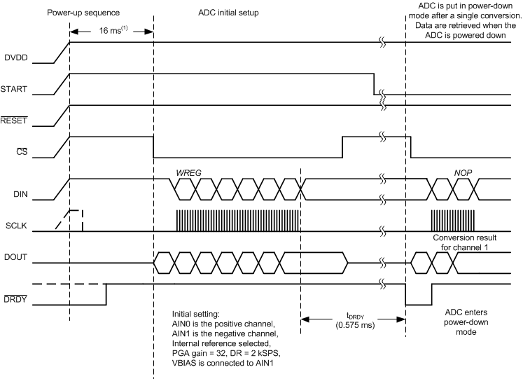
This second example deals with performing one conversion after power up and then entering power-down mode. In this example, a sensor is connected to input channels AIN0 and AIN1. Commands to set up the device must occur at least 216 system clock cycles after powering up the device. The ADC operates at a data rate of 2 kSPS. The PGA gain is set to 32. VBIAS is connected to the negative terminal of the sensor (that is, channel AIN1). All these settings can be changed by performing a block write operation on the first four registers of the device. After performing the block write operation, the START pin can be taken low. The device enters the power-down mode as soon as DRDY goes low 0.575 ms after writing into the SYS0 register. The conversion result can be retrieved even after the device enters power-down mode by sending 16 SCLK pulses.
10.2 Typical Applications
10.2.1 Ratiometric 3-Wire RTD Measurement System
Figure 81 shows a 3-wire RTD application circuit with lead-wire compensation using the ADS1147. The two IDAC current sources integrated in the ADS1147 are used to implement the lead-wire compensation. One IDAC current source (IDAC1) provides excitation to the RTD element. The other current source (IDAC2) has the same current setting, providing cancellation of lead-wire resistance by generating a voltage drop across lead-wire resistance RLEAD2 equal to the voltage drop across RLEAD1. Because the voltage across the RTD is measured differentially at ADC pins AIN1 and AIN2, the voltages across the lead-wire resistances cancel. The ADC reference voltage (pins REFP0 and REFN0) is derived from the voltage across RREF with the currents from IDAC1 and IDAC2, providing ratiometric cancellation of current-source drift. RREF also level shifts the RTD signal to within the ADC specified common-mode input range.
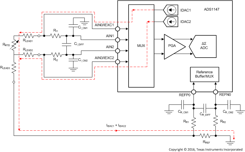 Figure 81. Ratiometric 3-Wire RTD Measurement System Featuring the ADS1147
10.2.1.1 Design Requirements
Table 42 shows the design requirements of the 3-wire RTD application.
Table 42. 3-Wire RTD Application Requirements
| PARAMETER | VALUE |
|---|---|
| Supply voltage | 3.3 V |
| Data rate | 20 SPS |
| RTD type | 3-wire PT100 |
| RTD excitation current | 1 mA |
| Temperature | –200°C to 850°C |
| Calibrated temperature measurement accuracy at TA = 25ºC(1) |
±0.2°C |
10.2.1.2 Detailed Design Procedure
10.2.1.2.1 Topology
Figure 82 shows the basic topology of a ratiometric measurement using an RTD. Shown are the ADC with the RTD and a reference resistor RREF. There is a single current source, labeled IDAC1 which is used to excite the RTD as well as to establish a reference voltage for the ADC across RREF.
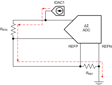 Figure 82. Example of a Ratiometric RTD Measurement
With IDAC1, the ADC measures the RTD voltage using the voltage across RREF as the reference. This gives a measurement such that the output code is proportional to the ratio of the RTD voltage and the reference voltage as shown in Equation 21 and Equation 22.
The currents cancel so that the equation reduces to Equation 23:
As shown in Equation 23, the measurement depends on the resistive value of the RTD and the reference resistor RREF, but not on the IDAC1 current value. Therefore, the absolute accuracy and temperature drift of the excitation current does not matter. This is a ratiometric measurement. As long as there is no current leakage from IDAC1 outside of this circuit, the measurement depends only on RRTD and RREF.
In Figure 83, the lead resistances of a 3-wire RTD are shown and another excitation current source is added, labeled IDAC2.
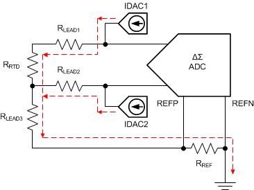 Figure 83. Example of Lead Wire Compensation
With a single excitation current source, RLEAD1 adds an error to the measurement. By adding IDAC2, the second excitation current source is used to cancel out the error in the lead wire resistance. When adding the lead resistances and the second current source, the equation becomes:
If the lead resistances match and the excitation currents match, then RLEAD1 = RLEAD2 and IIDAC1 = IIDAC2. The lead wire resistances cancel out so that Equation 24 reduces to the result in Equation 25 maintaining a ratiometric measurement.
RLEAD3 is not part of the measurement, because it is not in the input measurement path or in the reference input path.
As Equation 24 shows, the two current sources must be matched to cancel the lead resistances of the RTD wires. Any mismatch in the two current sources is minimized by using the multiplexer to swap or chop the two current sources between the two inputs. Taking measurements in both configurations and averaging the readings reduces the effects of mismatched current sources. The design uses the multiplexer in the ADS1147 to implement this chopping technique to remove the mismatch error between IDAC1 and IDAC2.
10.2.1.2.2 RTD Selection
The RTD is first chosen to be a PT100 element. The RTD resistance is defined by the Callendar-Van Dusen (CVD) equations and the resistance of the RTD is known depending on the temperature. The PT100 RTD has an impedance of 100 Ω at 0˚C and roughly 0.385 Ω of resistance change per 1˚C in temperature change. With a desired temperature measurement accuracy of 0.2˚C, this translates to a resistive measurement accuracy of approximately 0.077 Ω. The RTD resistance at the low end of the temperature range of –200˚C is 18.59 Ω and the resistance at the high end of the temperature range of 850˚C is 390.48 Ω.
10.2.1.2.3 Excitation Current
For the best possible resolution, the voltage across the RTD must be made as large as possible compared to the noise floor in the measurement. In general, measurement resolution improves with increasing excitation current. However, a larger excitation current creates self-heating in the RTD, which causes drift and error in the measurement. The selection of excitation currents trades off resolution against sensor self-heating.
The excitation current sources in this design are selected to be 1 mA. This maximizes the value of the RTD voltage while keeping the self-heating low. The typical range of RTD self-heating coefficients is 2.5 mW/°C for small, thin-film elements and 65 mW/°C for larger, wire-wound elements. With 1-mA excitation at the maximum RTD resistance value, the power dissipation in the RTD is less than 0.4 mW and keeps the measurement errors due to self-heating to less than 0.01˚C.
As mentioned in the Topology section, chopping of the excitation current sources cancels mismatches between the IDACs. This technique is necessary for getting the best possible accuracy from the system. Mismatch between the excitation current sources is a large source of error if chopping is not implemented.
The internal reference voltage must be enabled while using the IDACs, even if an external ratiometric measurement is used for ADC conversions.
Table 43 shows the ADS1147 register settings for setting up the internal reference and the excitation current sources.
Table 43. Register Bit Settings for Excitation Current Sources
| REGISTER (ADDRESS) | BIT NAME | BIT VALUES | COMMENT |
|---|---|---|---|
| MUX1 (02h)(1) | VREFCON[1:0] | 01 | Internal reference enabled |
| MUX1 (02h) | REFSELT[1:0] | 00 | REFP0 and REFN0 reference inputs selected |
| IDAC0 (0Ah) | IMAG[2:0] | 110 | IDAC magnitude = 1 mA |
| IDAC1 (0Bh) | I1DIR[3:0](2) | 0000 | IDAC1 = AIN0 |
| IDAC1 (0Bh) | I2DIR[3:0](2) | 0011 | IDAC2 = AIN3 |
10.2.1.2.4 Reference Resistor, RREF
TI recommends setting the common-mode voltage of the measurement near mid-supply, this helps keep the input within the common-mode input range of the PGA.
The reference resistor is selected to be 820 Ω. The voltage across RREF is calculated from Equation 26.
With AVDD = 3.3 V, Equation 26 shows that the input voltage is just below mid-supply.
The excitation current sources operate properly to a maximum IDAC compliance voltage. Above this compliance voltage, the current sources lose current regulation. In this example, the output voltage of the excitation current source is calculated from the sum of the voltages across the RTD and RREF as shown in Equation 27.
A compliance voltage of 3.3 V – 2.04 V = 1.26 V is sufficient for proper IDAC operation. See Figure 9 and Figure 10 in the Typical Characteristics section for details.
Because the voltage across RREF sets the reference voltage for the ADC, the tolerance and temperature drift of RREF directly affect the measurement gain. A resistor with 0.01% maximum tolerance is selected for this measurement.
10.2.1.2.5 PGA Setting
Because the excitation current is small to reduce self-heating, the PGA in the ADS1147 is used to amplify the signal across the RTD to use the full-scale range of the ADC. Starting with the reference voltage, the ADC is able to measure a differential input signal range of ±1.64 V. The maximum allowable PGA gain setting is based on the reference voltage, the maximum RTD resistance, and the excitation current.
As mentioned previously, the maximum resistance of the RTD is seen at the top range of the temperature measurement at 850°C. This gives the largest voltage measurement of the ADC. RRTD@850°C is 390.48 Ω.
With a reference voltage of 1.64 V, the maximum gain for the PGA, without over-ranging the ADC, is shown in Equation 29.
Selecting a PGA gain of 4 gives a maximum measurement of 95% of the positive full-scale range. Table 44 shows the register settings to set the PGA gain as well as the inputs for the ADC.
Table 44. Register Bit Settings for the Input Multiplexer and PGA
| REGISTER (ADDRESS) | BIT NAME | BIT VALUES | COMMENT |
|---|---|---|---|
| MUX0 (01h) | MUX_SP[2:0] | 001 | AINP = AIN1 |
| MUX0 (01h) | MUX_SN[2:0] | 010 | AINN = AIN2 |
| SYS0 (03h) | PGA[2:0] | 010 | PGA Gain = 4 |
10.2.1.2.6 Common-Mode Input Range
Now that the component values are selected, the common-mode input range must be verified to ensure that the ADC and PGA are not limited in operation. Start with the maximum input voltage, which gives the most restriction in the common-mode input range. At the maximum input voltage, the common-mode input voltage seen by the ADC is shown in Equation 30.
As mentioned in the Low-Noise PGA section, the common-mode input range is shown in Equation 3 and is applied to Equation 31.
After substituting in the appropriate values, the common-mode input range can be found in Equation 32 and Equation 33.
Because VCM = 1.835 V is within the limits of Equation 33, the RTD measurement is within the input common-mode range of the ADC and PGA. At the RTD voltage minimum (VRTD MIN = 18.59 mV), a similar calculation can be made to show that the input common-mode voltage is within the range as well.
10.2.1.2.7 Input and Reference Low-Pass Filters
The differential filters chosen for this application are designed to have a –3-dB corner frequency at least 10 times larger than the bandwidth of the ADC. The selected ADS1147 sampling rate of 20 SPS results in a –3-dB bandwidth of 14.8 Hz. The –3-dB filter corner frequency is set to be roughly 250 Hz at mid-scale measurement resistance. For proper operation, the differential cutoff frequencies of the reference and input low-pass filters must be well matched. This can be difficult because as the resistance of the RTD changes over the span of the measurement, the filter cutoff frequency changes as well. To mitigate this effect, the two resistors used in the input filter (RI1 and RI2) are chosen to be two orders of magnitude larger than the RTD. Input bias currents of the ADC causes a voltage drop across the filter resistors that shows up as a differential offset error if the bias currents and/or filter resistors are not equal. TI recommends limiting the resistors to at most 10 kΩ to reduce DC offset errors due to input bias current. RI1 and RI2 are chosen to be 4.7 kΩ.
The input filter differential capacitor (CI_DIFF) is calculated starting from the cutoff frequency as shown in Equation 34.
After solving for CI_DIFF, the capacitor is chosen to be a standard value of 68 nF.
To ensure that mismatch of the common-mode filter capacitors does not translate to a differential voltage, the common-mode capacitors (CI_CM1 and CI_CM2) are chosen to be 10 times smaller than the differential capacitor, making them 6.8 nF each. This results in a common-mode cutoff frequency that is roughly 20 times larger than the differential filter, making the matching of the common-mode cutoff frequencies less critical.
After substituting values into Equation 36 and Equation 37, the common-mode cutoff frequencies are found to be f–3dB_CM+ = 4.13 kHz and f–3dB_CM– = 4.24 kHz.
Often, filtering the reference input is not necessary and adding bulk capacitance at the reference input is sufficient. However, equations showing a design procedure calculating filter values for the reference inputs are shown below.
The differential reference filter is designed to have a –3-dB corner frequency of 250 Hz to match the differential input filter. The two reference filter resistors are selected to be 9.09 kΩ, several times larger than the value of RREF. The reference filter resistors must not be sized larger than 10 kΩ or DC bias errors become significant. The differential capacitor for the reference filter is calculated as shown in Equation 38.
After solving for CR_DIFF, the capacitor is chosen to be a standard value of 33 nF.
To ensure that mismatch of the common-mode filter capacitors does not translate to a differential voltage, the reference common-mode capacitors (CR_CM1 and CR_CM2) are chosen to be 10 times smaller than the reference differential capacitor, making them 3.3 nF each. Again, the resulting cutoff frequency for the common-mode filters is roughly 20 times larger than the differential filter, making the matching of the cutoff frequencies less critical.
After substituting values into Equation 40 and Equation 41, common-mode cutoff frequencies for the reference filter are found to be f–3dB_CM+ = 4.87 kHz and f–3dB_CM+ = 5.31 kHz.
10.2.1.2.8 Register Settings
The register settings for this design are shown in Table 45.
Table 45. Register Settings
| REGISTER | NAME | SETTING | DESCRIPTION |
|---|---|---|---|
| 00h | MUX0 | 0Ah | Select AINP = AIN1 and AINN = AIN2 |
| 01h | VBIAS | 00h | |
| 02h | MUX1 | 20h | Internal reference enabled, REFP0 and REFN0 reference inputs selected |
| 03h | SYS0 | 22h | PGA Gain = 4, DR = 20 SPS |
| 04h | OFC0(1) | xxh | |
| 05h | OFC1 | xxh | |
| 06h | OFC2 | xxh | |
| 07h | FSC0(1) | xxh | |
| 08h | FSC1 | xxh | |
| 09h | FSC2 | xxh | |
| 0Ah | IDAC0 | x6h | ID bits may be version dependent, IDAC magnitude set to 1 mA |
| 0Bh | IDAC1 | 03h(2) | IDAC1 set to AIN0; IDAC2 set to AIN3 |
| 0Ch | GPIOCFG | 00h | |
| 0Dh | GPIOCDIR | 00h | |
| 0Eh | GPIODAT | 00h |
10.2.1.3 Application Curves
To test the accuracy of the acquisition circuit, a series of calibrated, high-precision discrete resistors are used as the input to the system. Measurements are taken at TA = 25°C. Figure 84 displays the uncalibrated resistance measurement accuracy of the system over an input span from 20 Ω to 400 Ω. For each resistor value, 512 measurements are taken. With each measurement, IDAC1 and IDAC2 are chopped to remove the excitation current mismatch.
The uncalibrated measurement error is displayed in Figure 85. The offset and gain error can be primarily attributed to the offset and gain error of the ADC. However, the accuracy of RREF contributes directly to the accuracy of the measurement. To keep the gain error low, RREF must be a low-drift precision resistor.
Precision temperature measurement applications are typically calibrated to remove the effects of gain and offset errors, which generally dominate the total system error. The simplest calibration method is a linear, or two-point, calibration which applies an equal and opposite gain and offset term to cancel the measured system gain and offset errors. Using the results of Figure 85, the uncalibrated gain and offset error are then used to modify the Offset Calibration and the Full-Scale Calibration registers in the device. The results of this calibrated system measurement are shown in Figure 86.
The results in Figure 86 are converted to temperature accuracy by dividing the results by the RTD sensitivity (α) at the measured resistance. Over the full resistance input range, the maximum total measured error is
±0.011 Ω. Equation 42 uses the measured resistance error and the nominal RTD sensitivity to calculate the measured temperature accuracy.

Figure 87 displays the calculated temperature measurement accuracy of the circuit assuming a linear RTD resistance to temperature response. It does not include any linearity compensation of the RTD.
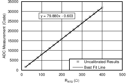 Figure 84. Resistance Measurement Results With Precision Resistors Before Calibration
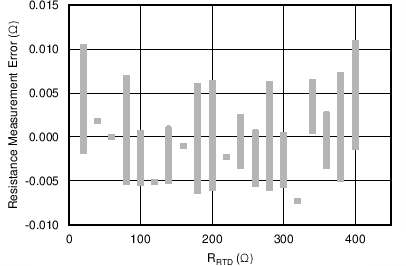 Figure 86. Resistance Measurement Error With Precision Resistors After Calibration
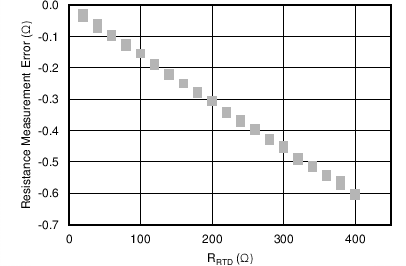 Figure 85. Resistance Measurement Error With Precision Resistors Before Calibration
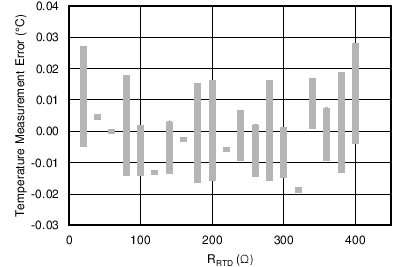 Figure 87. Calculated Temperature Measurement Error from Resistance Measurement Error
Table 46 compares the measurement accuracy with the design goal from Table 42.
Table 46. Comparison of Design Goals and Measured Performance
| GOAL | MEASURED | ||
|---|---|---|---|
| Calibrated resistance measurement accuracy at TA = 25ºC | ±0.077 Ω | ±0.011 Ω | |
| Calibrated temperature measurement accuracy at TA = 25ºC | ±0.2°C | ±0.029°C | |
10.2.2 K-Type Thermocouple Measurement (–200°C to 1250°C) With Cold-Junction Compensation
Figure 88 shows the basic connections of a thermocouple measurement system based on the ADS1148. This circuit uses a cold-junction compensation measurement based on the Ratiometric 3-Wire RTD Measurement System topology shown in the previous application example. Using the IEXC1 and IEXC2 pins allow for routing of the IDAC currents without using any other analog pins. Along with the thermocouple and cold-junction measurements, four other analog inputs (AIN4 to AIN7 not shown in the schematic) are available for alternate measurements or use as GPIO pins.
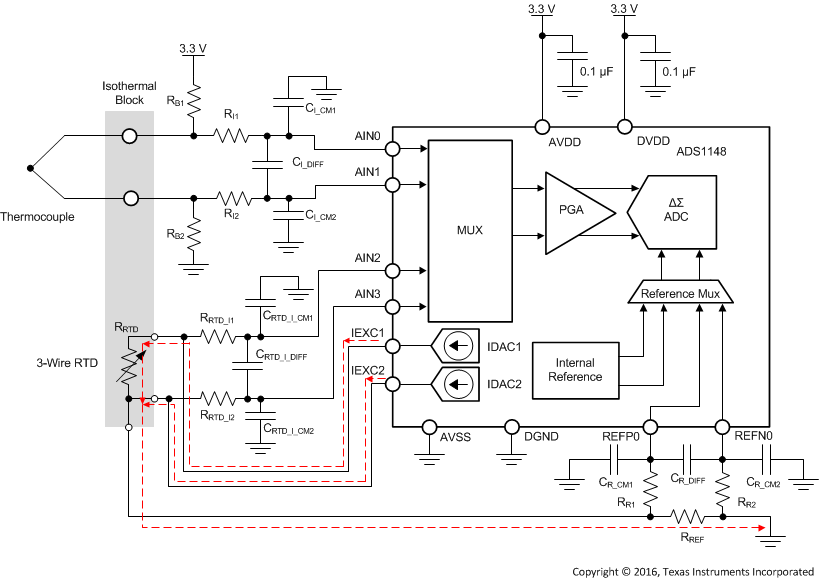 Figure 88. Thermocouple Measurement System Using the ADS1148
10.2.2.1 Design Requirements
Table 47 shows the design requirements of the thermocouple application for the ADS1148.
Table 47. Example Thermocouple Application Requirements
| PARAMETER | VALUE |
|---|---|
| Supply voltage | 3.3 V |
| Reference voltage | Internal 2.048-V reference |
| Update rate | ≥ 10 readings per second |
| Thermocouple type | K |
| Temperature measurement | –200ºC to 1250ºC |
| Measurement accuracy at TA = 25ºC(1) | ±0.5ºC |
10.2.2.2 Detailed Design Procedure
10.2.2.2.1 Biasing Resistors
The biasing resistors RB1 and RB2 are used to set the common-mode voltage of the thermocouple to within the specified common-mode voltage range of the PGA (in this example, to mid-supply AVDD / 2). If the application requires the thermocouple to be biased to GND, a bipolar supply (for example, AVDD = 2.5 V and AVSS =
–2.5 V) must be used for the device to meet the common-mode voltage requirement of the PGA. When choosing the values of the biasing resistors, care must be taken so that the biasing current does not degrade measurement accuracy. The biasing current flows through the thermocouple and can cause self-heating and additional voltage drops across the thermocouple leads. Typical values for the biasing resistors range from 1 MΩ to 50 MΩ.
In addition to biasing the thermocouple, RB1 and RB2 are also useful for detecting an open thermocouple lead. When one of the thermocouple leads fails open, the biasing resistors pull the analog inputs (AIN0 and AIN1) to AVDD and AVSS, respectively. The ADC consequently reads a full-scale value, which is outside the normal measurement range of the thermocouple voltage, to indicate this failure condition.
10.2.2.2.2 Input Filtering
Although the digital filter attenuates high-frequency components of noise, TI recommends providing a first-order, passive RC filter at the inputs to further improve performance. The differential RC filter formed by RI1, RI2, and the differential capacitor CI_DIFF offers a cutoff frequency that is calculated using Equation 43.
Two common-mode filter capacitors (CI_CM1 and CI_CM2) are also added to offer attenuation of high-frequency, common-mode noise components. TI recommends that the differential capacitor CI_DIFF be at least an order of magnitude (10×) larger than the common-mode capacitors (CI_CM1 and CI_CM2) because mismatches in the common-mode capacitors can convert common-mode noise into differential noise.
The filter resistors RF1 and RF2 also serve as current-limiting resistors. These resistors limit the current into the analog inputs (AIN0 and AIN1) of the device to safe levels if an overvoltage on the inputs occurs. Care must be taken when choosing the filter resistor values because the input currents flowing into and out of the device cause a voltage drop across the resistors. This voltage drop shows up as an additional offset error at the ADC inputs. For thermocouple measurements, TI recommends limiting the filter resistor values to below 10 kΩ.
The filter component values used in this design are: RI1 = RI2 = 1 kΩ, CI_DIFF = 100 nF, and CI_CM1 = CI_CM2 = 10 nF.
10.2.2.2.3 PGA Setting
The highest measurement resolution is achieved when matching the largest potential input signal to the FSR of the ADC by choosing the highest possible gain. From the design requirement, the maximum thermocouple voltage occurs at TTC = 1250°C and is VTC = 50.644 mV as defined in the tables published by the National Institute of Standards and Technology (NIST) using a cold-junction temperature of TCJ = 0°C. A thermocouple produces an output voltage that is proportional to the temperature difference between the thermocouple tip and the cold junction. If the cold junction is at a temperature below 0°C, the thermocouple produces a voltage larger than 50.644 mV. The isothermal block area is constrained by the operating temperature range of the device. Therefore, the isothermal block temperature is limited to –40°C. A K-type thermocouple at TTC = 1250°C produces an output voltage of VTC = 50.644 mV – (–1.527 mV) = 52.171 mV when referenced to a cold-junction temperature of TCJ = –40°C. The maximum gain that can be applied when using the internal 2.048-V reference is then calculated as 39.3 from Equation 44. The next smaller PGA gain setting the device offers is 32.
10.2.2.2.4 Cold-Junction Measurement
AIN2 and AIN3 are attached to a 3-wire RTD that is used to measure the cold-junction temperature. Similar to the example in the Ratiometric 3-Wire RTD Measurement System section, the 3-wire RTD design is the same except the inputs and excitation current sources have been changed. Note that RREF and PGA Gain can be optimized for a reduced temperature range.
The device does not perform an automatic cold-junction compensation of the thermocouple. This compensation must be done in the microcontroller that interfaces to the device. The microcontroller requests one or multiple readings of the thermocouple voltage from the device and then sets the device to measure the cold junction with the RTD to compensate for the cold-junction temperature.
An algorithm similar to the following must be implemented on the microcontroller to compensate for the cold-junction temperature:
- Measure the thermocouple voltage, V(TC), between AIN0 and AIN1.
- Measure the temperature of the cold junction, T(CJ), using a ratiometric measurement with the 3-wire RTD across AIN2 and AIN3.
- Convert the cold-junction temperature into an equivalent thermoelectric voltage, V(CJ), using the tables or equations provided by NIST.
- Add V(TC) and V(CJ) and translate the summation back into a thermocouple temperature using the NIST tables or equations again.
There are alternate methods of measuring the cold-junction temperature. The additional analog input channels of the device can be used in this case to measure the cold-junction temperature with a thermistor or an alternate analog temperature sensor.
10.2.2.2.5 Calculated Resolution
To get an approximation of the achievable temperature resolution, the peak-to-peak noise of the ADS1148 at Gain = 32 and DR = 20 SPS (1.95 µVPP) is taken from Table 1. The noise is divided by the average sensitivity of a K-type thermocouple (41 µV/°C), as shown in Equation 45.
10.2.2.2.6 Register Settings
The register settings for this design are shown in Table 48. The inputs are selected to measure the thermocouple and the internal reference is enabled and selected. The excitation current sources are also enabled and selected. While this does consume some power, it allows for a quick transition for the cold-junction measurement.
Table 48. Register Settings for the Thermocouple Measurement
| REGISTER | NAME | SETTING | DESCRIPTION |
|---|---|---|---|
| 00h | MUX0 | 01h | Select AINP = AIN0, AINN = AIN1 |
| 01h | VBIAS | 00h | |
| 02h | MUX1 | 30h | Internal reference enabled, internal reference selected |
| 03h | SYS0 | 52h | PGA Gain = 32, DR = 20 SPS |
| 04h | OFC0 | xxh | |
| 05h | OFC1 | xxh | |
| 06h | OFC2 | xxh | |
| 07h | FSC0 | xxh | |
| 08h | FSC1 | xxh | |
| 09h | FSC2 | xxh | |
| 0Ah | IDAC0 | x6h | IDAC magnitude set to 1 mA |
| 0Bh | IDAC1 | 89h | IDAC1 set to IEXC1, IDAC2 set to IEXC2 |
| 0Ch | GPIOCFG | 00h | |
| 0Dh | GPIOCDIR | 00h | |
| 0Eh | GPIODAT | 00h |
Changing to the cold-junction measurement, the registers are set to measure the RTD. This requires changing the input, the reference input, the gain, and any calibration settings required for the measurement accuracy. Table 49 shows the register settings for the RTD measurement used for cold-junction compensation.
Table 49. Register Settings for the Cold-Junction Measurement
| REGISTER | NAME | SETTING | DESCRIPTION |
|---|---|---|---|
| 00h | MUX0 | 13h | Select AINP = AIN2, AINN = AIN3 |
| 01h | VBIAS | 00h | |
| 02h | MUX1 | 20h | Internal reference enabled, REFP0 and REFN0 selected |
| 03h | SYS0 | 22h | PGA Gain = 4, DR = 20 SPS |
| 04h | OFC0 | xxh | Calibration values are different between measurement settings |
| 05h | OFC1 | xxh | |
| 06h | OFC2 | xxh | |
| 07h | FSC0 | xxh | |
| 08h | FSC1 | xxh | |
| 09h | FSC2 | xxh | |
| 0Ah | IDAC0 | x6h | IDAC magnitude set to 1 mA |
| 0Bh | IDAC1 | 89h | IDAC1 set to IEXC1, IDAC2 set to IEXC2 |
| 0Ch | GPIOCFG | 00h | |
| 0Dh | GPIOCDIR | 00h | |
| 0Eh | GPIODAT | 00h |
10.3 Do's and Don'ts
- Do partition the analog, digital, and power supply circuitry into separate sections on the PCB.
- Do use a single ground plane for analog and digital grounds.
- Do place the analog components close to the ADC pins using short, direct connections.
- Do keep the SCLK pin free of glitches and noise.
- Do verify that the analog input voltages are within the specified PGA input voltage range under all input conditions.
- Do float unused analog input pins to minimize input leakage current. Connecting unused pins to AVDD is the next best option.
- Do provide current limiting to the analog inputs in case overvoltage faults occur.
- Do use a low-dropout linear regulator (LDO) to reduce ripple voltage generated by switch-mode power supplies. This is especially true for AVDD where the supply noise may affect the performance.
- Don't cross analog and digital signals.
- Don't allow the analog and digital power supply voltages to exceed 5.5 V under all conditions, including during power up and power down.
Figure 89 shows Do's and Don'ts of ADC circuit connections.
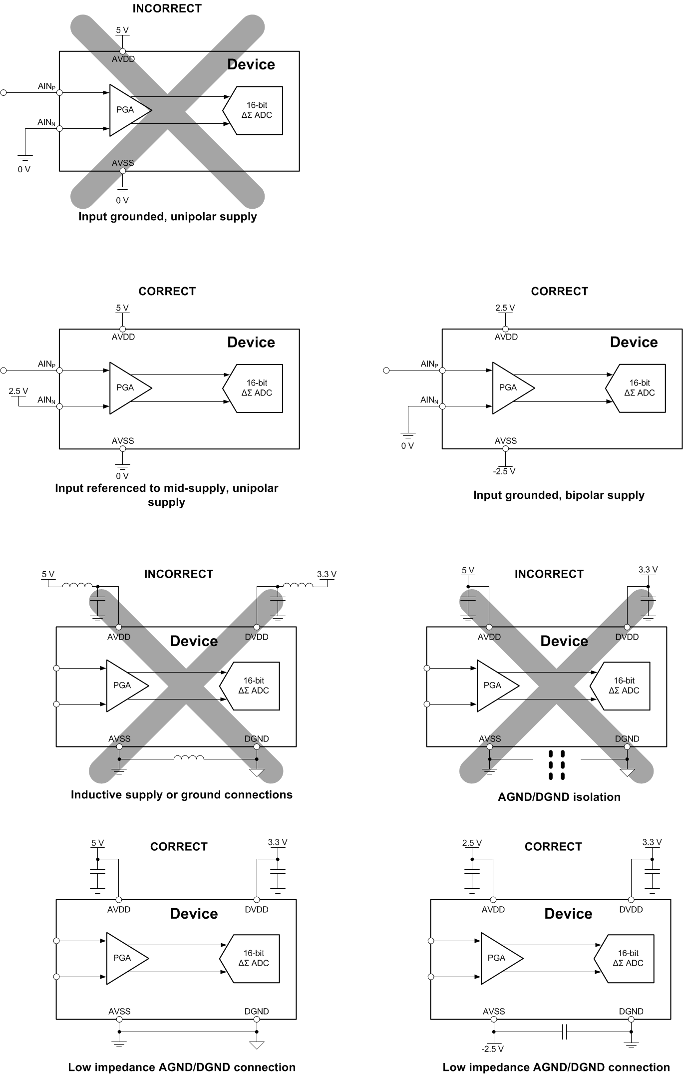 Figure 89. Do's and Don'ts Circuit Connections
