JAJS168G June 2005 – January 2021 ADS1232 , ADS1234
PRODUCTION DATA
- 1 特長
- 2 アプリケーション
- 3 概要
- 4 Revision History
- 5 Pin Configuration and Functions
- 6 Specifications
- 7 Parameter Measurement Information
-
8 Detailed Description
- 8.1 Overview
- 8.2 Functional Block Diagram
- 8.3
Feature Description
- 8.3.1 Analog Inputs (AINPX, AINNX)
- 8.3.2 Temperature Sensor (ADS1232 Only)
- 8.3.3 Low-Noise PGA
- 8.3.4 Voltage Reference Inputs (REFP, REFN)
- 8.3.5 Clock Sources
- 8.3.6 Digital Filter Frequency Response
- 8.3.7 Settling Time
- 8.3.8 Data Rate
- 8.3.9 Data Format
- 8.3.10 Data Ready and Data Output (DRDY/DOUT)
- 8.3.11 Serial Clock Input (SCLK)
- 8.3.12 Data Retrieval
- 8.4 Device Functional Modes
- 9 Application and Implementation
- 10Power Supply Recommendations
- 11Layout
- 12Device and Documentation Support
- 13Mechanical, Packaging, and Orderable Information
8.3.2 Temperature Sensor (ADS1232 Only)
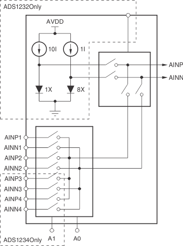
On-chip diodes provide temperature-sensing capability. By setting the TEMP pin high, the selected analog inputs are disconnected and the inputs to the ADC are connected to the anodes of two diodes scaled to 1x and 80x in current and size, as shown in Figure 8-1. By measuring the difference in voltage of these diodes, temperature changes can be inferred from a baseline temperature. Typically, the difference in diode voltage is 111.7 mV at 25°C with a temperature coefficient of 379 µV/°C. With PGA gain = 1 and 2, the difference voltage output from the PGA is 111.7 mV and 223.4 mV, respectively. The temperature sensor function is impossible to use with PGA gain = 64 and 128.
 Figure 8-1 Measurement of the Temperature Sensor in the Input Multiplexer