JAJS168G June 2005 – January 2021 ADS1232 , ADS1234
PRODUCTION DATA
- 1 特長
- 2 アプリケーション
- 3 概要
- 4 Revision History
- 5 Pin Configuration and Functions
- 6 Specifications
- 7 Parameter Measurement Information
-
8 Detailed Description
- 8.1 Overview
- 8.2 Functional Block Diagram
- 8.3
Feature Description
- 8.3.1 Analog Inputs (AINPX, AINNX)
- 8.3.2 Temperature Sensor (ADS1232 Only)
- 8.3.3 Low-Noise PGA
- 8.3.4 Voltage Reference Inputs (REFP, REFN)
- 8.3.5 Clock Sources
- 8.3.6 Digital Filter Frequency Response
- 8.3.7 Settling Time
- 8.3.8 Data Rate
- 8.3.9 Data Format
- 8.3.10 Data Ready and Data Output (DRDY/DOUT)
- 8.3.11 Serial Clock Input (SCLK)
- 8.3.12 Data Retrieval
- 8.4 Device Functional Modes
- 9 Application and Implementation
- 10Power Supply Recommendations
- 11Layout
- 12Device and Documentation Support
- 13Mechanical, Packaging, and Orderable Information
8.3.5 Clock Sources
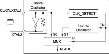
The ADS123x can use an external clock source, external crystal, or internal oscillator to accommodate a wide variety of applications. Figure 8-4 shows the equivalent circuitry of the clock source. The CLK_DETECT block determines whether a crystal oscillator or external clock signal is applied to the CLKIN/XTAL1 pin so that the internal oscillator is bypassed or activated. When the CLKIN/XTAL1 pin frequency is above approximately 200 kHz, the CLK_DETECT output goes low and shuts down the internal oscillator. When the CLKIN/XTAL1 pin frequency is below approximately 200 kHz, the CLK_DETECT output goes high and activates the internal oscillator. Connect the CLKIN/XTAL1 pin to ground when the internal oscillator is chosen.
 Figure 8-4 Equivalent Circuitry of the Clock Source
For crystal operation, connect the 4.9152-MHz crystal across the CLKIN/XTAL1 and XTAL2 pins. Table 8-4 shows the recommended crystal part numbers. As a result of the low-power design of the internal parallel-resonant circuit, both the CLKIN/XTAL1 and XTAL2 pins are only for use with the external crystal; do not use these pins as clock output drivers for external circuitry. No external capacitors are used with the crystal. Place the crystal as close as possible to the device pins in order to reduce board stray capacitance and in order to help ensure proper crystal operation.
| MANUFACTURER | FREQUENCY | PART NUMBER |
|---|---|---|
| ECS | 4.9152 MHz | ECS-49-20-1 |
| ECS | 4.9152 MHz | ECS-49-20-4 |
An external clock oscillator can be used by driving the CLKIN/XTAL1 pin from the oscillator output and leave XTAL2 disconnected.