JAJSGG2C October   2018  – June 2019 ADS125H02

PRODUCTION DATA.  

  1. 特長
  2. アプリケーション
  3. 概要
    1.     機能ブロック図
  4. 改訂履歴
  5. 概要(続き)
  6. Device Comparison Table
  7. Pin Configuration and Functions
    1.     Pin Functions
  8. Specifications
    1. 8.1 Absolute Maximum Ratings
    2. 8.2 ESD Ratings
    3. 8.3 Recommended Operating Conditions
    4. 8.4 Thermal Information
    5. 8.5 Electrical Characteristics
    6. 8.6 Timing Requirements
    7. 8.7 Switching Characteristics
    8. 8.8 Typical Characteristics
  9. Parameter Measurement Information
    1. 9.1 Noise Performance
  10. 10Detailed Description
    1. 10.1 Overview
    2. 10.2 Functional Block Diagram
    3. 10.3 Feature Description
      1. 10.3.1 Input Range
      2. 10.3.2 Analog Inputs
        1. 10.3.2.1 ESD Diodes
        2. 10.3.2.2 Input Multiplexer
          1. 10.3.2.2.1 Analog Inputs (AIN0, AIN1, AINCOM)
          2. 10.3.2.2.2 High-Voltage Power Supply Readback
          3. 10.3.2.2.3 Internal VCOM Connection (Default)
          4. 10.3.2.2.4 Temperature Sensor
      3. 10.3.3 Programmable Gain Amplifier (PGA)
        1. 10.3.3.1 PGA Operating Range
        2. 10.3.3.2 PGA Monitor
      4. 10.3.4 Reference Voltage
        1. 10.3.4.1 Internal Reference
        2. 10.3.4.2 External Reference
        3. 10.3.4.3 AVDD Power-Supply Reference
        4. 10.3.4.4 Reference Monitor
      5. 10.3.5 Current Sources (IDAC1 and IDAC2)
      6. 10.3.6 General-Purpose Inputs and Outputs (GPIOs)
      7. 10.3.7 ADC Modulator
      8. 10.3.8 Digital Filter
        1. 10.3.8.1 Sinc Filter Mode
          1. 10.3.8.1.1 Sinc Filter Frequency Response
        2. 10.3.8.2 FIR Filter
        3. 10.3.8.3 50-Hz and 60-Hz Normal Mode Rejection
    4. 10.4 Device Functional Modes
      1. 10.4.1 Conversion Control
        1. 10.4.1.1 Continuous-Conversion Mode
        2. 10.4.1.2 Pulse-Conversion Mode
        3. 10.4.1.3 Conversion Latency
        4. 10.4.1.4 Start-Conversion Delay
      2. 10.4.2 Auto-Zero Mode
      3. 10.4.3 Clock Mode
      4. 10.4.4 Reset
        1. 10.4.4.1 Power-On Reset
        2. 10.4.4.2 Reset by Pin
        3. 10.4.4.3 Reset by Command
      5. 10.4.5 Calibration
        1. 10.4.5.1 Offset and Full-Scale Calibration
          1. 10.4.5.1.1 Offset Calibration Registers
          2. 10.4.5.1.2 Full-Scale Calibration Registers
        2. 10.4.5.2 Offset Calibration (OFSCAL)
        3. 10.4.5.3 Full-Scale Calibration (GANCAL)
        4. 10.4.5.4 Calibration Command Procedure
        5. 10.4.5.5 User Calibration Procedure
    5. 10.5 Programming
      1. 10.5.1 Serial Interface
        1. 10.5.1.1 Chip-Select Pins (CS1 and CS2)
        2. 10.5.1.2 Serial Clock (SCLK)
        3. 10.5.1.3 Data Input (DIN)
        4. 10.5.1.4 Data Output/Data Ready (DOUT/DRDY)
      2. 10.5.2 Data Ready (DRDY)
        1. 10.5.2.1 DRDY in Continuous-Conversion Mode
        2. 10.5.2.2 DRDY in Pulse-Conversion Mode
        3. 10.5.2.3 Data Ready by Software Polling
      3. 10.5.3 Conversion Data
        1. 10.5.3.1 Status Byte (STATUS0)
        2. 10.5.3.2 Conversion Data Format
      4. 10.5.4 Cyclic Redundancy Check (CRC)
      5. 10.5.5 Commands
        1. 10.5.5.1  General Command Format
        2. 10.5.5.2  NOP Command
        3. 10.5.5.3  RESET Command
        4. 10.5.5.4  START Command
        5. 10.5.5.5  STOP Command
        6. 10.5.5.6  RDATA Command
        7. 10.5.5.7  OFSCAL Command
        8. 10.5.5.8  GANCAL Command
        9. 10.5.5.9  RREG Command
        10. 10.5.5.10 WREG Command
        11. 10.5.5.11 LOCK Command
        12. 10.5.5.12 UNLOCK Command
    6. 10.6 Register Map
      1. 10.6.1  Device Identification (ID) Register (address = 00h) [reset = 6xh]
        1. Table 30. ID Register Field Descriptions
      2. 10.6.2  Main Status (STATUS0) Register (address = 01h) [reset = 01h]
        1. Table 31. STATUS0 Register Field Descriptions
      3. 10.6.3  Mode 0 (MODE0) Register (address = 02h) [reset = 24h]
        1. Table 32. MODE0 Register Field Descriptions
      4. 10.6.4  Mode 1 (MODE1) Register (address = 03h) [reset = 01h]
        1. Table 33. MODE1 Register Field Descriptions
      5. 10.6.5  Mode 2 (MODE2) Register (address = 04h) [reset = 00h]
        1. Table 34. MODE2 Register Field Descriptions
      6. 10.6.6  Mode 3 (MODE3) Register (address = 05h) [reset = 00h]
        1. Table 35. MODE3 Register Field Descriptions
      7. 10.6.7  Reference Configuration (REF) Register (address = 06h) [reset = 05h]
        1. Table 36. REF Register Field Descriptions
      8. 10.6.8  Offset Calibration (OFCALx) Registers (address = 07h, 08h, 09h) [reset = 00h, 00h, 00h]
        1. Table 37. OFCAL0, OFCAL1, OFCAL2 Registers Field Description
      9. 10.6.9  Full-Scale Calibration (FSCALx) Registers (address = 0Ah, 0Bh, 0Ch) [reset = 00h, 00h, 40h]
        1. Table 38. FSCAL0, FSCAL1, FSCAL2 Registers Field Description
      10. 10.6.10 Current Source Multiplexer (I_MUX) Register (address = 0Dh) [reset = FFh]
        1. Table 39. I_MUX Register Field Descriptions
      11. 10.6.11 Current Source Magnitude (I_MAG) Register (address = 0Eh) [reset = 00h]
        1. Table 40. I_MAG Register Field Descriptions
      12. 10.6.12 Reserved (RESERVED) Register (address = 0Fh) [reset = 00h]
        1. Table 41. RESERVED Register Field Descriptions
      13. 10.6.13 MODE4 (MODE4) Register (address = 10h) [reset = 50h]
        1. Table 42. MODE4 Register Field Descriptions
      14. 10.6.14 PGA Alarm (STATUS1) Register (address = 11h) [reset = xxh]
        1. Table 43. STATUS1 Register Field Descriptions
      15. 10.6.15 Status 2 (STATUS2) Register (address = 12h) [reset = 0xh]
        1. Table 44. STATUS2 Register Field Descriptions
  11. 11Application and Implementation
    1. 11.1 Application Information
      1. 11.1.1 Input Range
      2. 11.1.2 Input Overload
        1. 11.1.2.1 Input Signal Rate of Change (dV/dt)
      3. 11.1.3 Unused Inputs and Outputs
    2. 11.2 Typical Applications
      1. 11.2.1 ±10-V Analog Input Module
        1. 11.2.1.1 Design Requirements
        2. 11.2.1.2 Detailed Design Procedure
        3. 11.2.1.3 Application Curves
      2. 11.2.2 Thermocouple Input With High Common-Mode Voltage
    3. 11.3 Initialization Setup
  12. 12Power Supply Recommendations
    1. 12.1 Power-Supply Decoupling
    2. 12.2 Analog Power-Supply Clamp
    3. 12.3 Power-Supply Sequencing
    4. 12.4 5-V to ±15-V DC-DC Converter
  13. 13Layout
    1. 13.1 Layout Guidelines
    2. 13.2 Layout Example
  14. 14デバイスおよびドキュメントのサポート
    1. 14.1 ドキュメントのサポート
      1. 14.1.1 関連資料
    2. 14.2 ドキュメントの更新通知を受け取る方法
    3. 14.3 コミュニティ・リソース
    4. 14.4 商標
    5. 14.5 静電気放電に関する注意事項
    6. 14.6 Glossary
  15. 15メカニカル、パッケージ、および注文情報

パッケージ・オプション

メカニカル・データ(パッケージ|ピン)
サーマルパッド・メカニカル・データ
発注情報

PGA Monitor

The PGA requires operating voltage headroom at the input and output nodes. The PGA must be within the linear operating range, otherwise the conversion data are not valid. Use the internal PGA monitors to assist in the detection of PGA overload. The PGA has four monitors (two monitors for the input and two monitors for the output) with high and low thresholds for each, for a total of eight possible alarms. The status of each PGA monitor is read in the STATUS1 register. The PGA monitoring points are illustrated in Figure 57. Figure 60 shows the operation of the low-overload threshold and the high-overload threshold of each PGA monitor point.
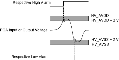
ADS125H02 ads125h02-PGA-overload-threshold.gifFigure 60. PGA Monitor Thresholds

Check for PGA overload by polling the STAT12 bit (bit 4 of the STATUS conversion byte or STATUS0 register). The STAT12 bit is the logical OR of all PGA error flags with the CRC-2 error flag. After the STAT12 bit asserts, poll the STATUS1 and STATUS2 registers (address 11h and 12h) to determine the source of the error. The status of the PGA overload is latched in the STATUS1 register and remains latched after the overload condition is removed. Reading the STATUS1 register clears the PGA overload bits (clear-on-read operation). The PGA overload flags and the CRC2 flag must be reset in order to clear the STAT12 bit. See the STATUS1 register for a description of the PGA overload bits.

The PGA monitors are analog comparators that can respond to transient overload conditions. Transient conditions can occur, for example, when multiplexing the inputs or when the gain is too high for the voltage of the next channel.