JAJSGW2A January   2019  – May 2019 ADS1260-Q1 , ADS1261-Q1

PRODUCTION DATA.  

  1. 特長
  2. アプリケーション
  3. 概要
    1.     Device Images
      1.      ブロック図
  4. 改訂履歴
  5. 概要(続き)
  6. Device Comparison Table
  7. Pin Configuration and Functions
    1.     Pin Functions
  8. Specifications
    1. 8.1 Absolute Maximum Ratings
    2. 8.2 ESD Ratings
    3. 8.3 Recommended Operating Conditions
    4. 8.4 Thermal Information
    5. 8.5 Electrical Characteristics
    6. 8.6 Timing Requirements
    7. 8.7 Switching Characteristics
  9. Parameter Measurement Information
    1. 9.1 Noise Performance
  10. 10Detailed Description
    1. 10.1 Overview
    2. 10.2 Functional Block Diagram
    3. 10.3 Feature Description
      1. 10.3.1  Analog Inputs
        1. 10.3.1.1 ESD Diodes
        2. 10.3.1.2 Input Multiplexer
        3. 10.3.1.3 Temperature Sensor
        4. 10.3.1.4 Power-Supply Readback
        5. 10.3.1.5 Inputs Open
        6. 10.3.1.6 Internal VCOM Connection
        7. 10.3.1.7 Alternate Functions
      2. 10.3.2  PGA
        1. 10.3.2.1 PGA Bypass Mode
        2. 10.3.2.2 PGA Voltage Monitor
      3. 10.3.3  Reference Voltage
        1. 10.3.3.1 Internal Reference
        2. 10.3.3.2 External Reference
        3. 10.3.3.3 AVDD - AVSS Reference (Default)
        4. 10.3.3.4 Reference Monitor
      4. 10.3.4  Level-Shift Voltage (VBIAS)
      5. 10.3.5  Burn-Out Current Sources
      6. 10.3.6  Sensor-Excitation Current Sources (IDAC1 and IDAC2)
      7. 10.3.7  General-Purpose Input/Outputs (GPIOs)
      8. 10.3.8  Oversampling
      9. 10.3.9  Modulator
      10. 10.3.10 Digital Filter
        1. 10.3.10.1 Sinc Filter
          1. 10.3.10.1.1 Sinc Filter Frequency Response
        2. 10.3.10.2 FIR Filter
          1. 10.3.10.2.1 FIR Filter Frequency Response
        3. 10.3.10.3 Filter Bandwidth
        4. 10.3.10.4 50-Hz and 60-Hz Normal Mode Rejection
    4. 10.4 Device Functional Modes
      1. 10.4.1 Conversion Control
        1. 10.4.1.1 Continuous-Conversion Mode
        2. 10.4.1.2 Pulse-Conversion Mode
        3. 10.4.1.3 Conversion Latency
        4. 10.4.1.4 Start-Conversion Delay
      2. 10.4.2 Chop Mode
      3. 10.4.3 AC-Excitation Mode
      4. 10.4.4 ADC Clock Mode
      5. 10.4.5 Power-Down Mode
        1. 10.4.5.1 Hardware Power-Down
        2. 10.4.5.2 Software Power-Down
      6. 10.4.6 Reset
        1. 10.4.6.1 Power-on Reset
        2. 10.4.6.2 Reset by Pin
        3. 10.4.6.3 Reset by Command
      7. 10.4.7 Calibration
        1. 10.4.7.1 Offset and Full-Scale Calibration
          1. 10.4.7.1.1 Offset Calibration Registers
          2. 10.4.7.1.2 Full-Scale Calibration Registers
        2. 10.4.7.2 Offset Self-Calibration (SFOCAL)
        3. 10.4.7.3 Offset System-Calibration (SYOCAL)
        4. 10.4.7.4 Full-Scale Calibration (GANCAL)
        5. 10.4.7.5 Calibration Command Procedure
        6. 10.4.7.6 User Calibration Procedure
    5. 10.5 Programming
      1. 10.5.1 Serial Interface
        1. 10.5.1.1 Chip Select (CS)
        2. 10.5.1.2 Serial Clock (SCLK)
        3. 10.5.1.3 Data Input (DIN)
        4. 10.5.1.4 Data Output/Data Ready (DOUT/DRDY)
        5. 10.5.1.5 Serial Interface Auto-Reset
      2. 10.5.2 Data Ready (DRDY)
        1. 10.5.2.1 DRDY in Continuous-Conversion Mode
        2. 10.5.2.2 DRDY in Pulse-Conversion Mode
        3. 10.5.2.3 Data Ready by Software Polling
      3. 10.5.3 Conversion Data
        1. 10.5.3.1 Status byte (STATUS)
        2. 10.5.3.2 Conversion Data Format
      4. 10.5.4 CRC
      5. 10.5.5 Commands
        1. 10.5.5.1  NOP Command
        2. 10.5.5.2  RESET Command
        3. 10.5.5.3  START Command
        4. 10.5.5.4  STOP Command
        5. 10.5.5.5  RDATA Command
        6. 10.5.5.6  SYOCAL Command
        7. 10.5.5.7  GANCAL Command
        8. 10.5.5.8  SFOCAL Command
        9. 10.5.5.9  RREG Command
        10. 10.5.5.10 WREG Command
        11. 10.5.5.11 LOCK Command
        12. 10.5.5.12 UNLOCK Command
    6. 10.6 Register Map
      1. 10.6.1  Device Identification (ID) Register (address = 00h) [reset = xxh]
        1. Table 30. ID Register Field Descriptions
      2. 10.6.2  Device Status (STATUS) Register (address = 01h) [reset = 01h]
        1. Table 31. STATUS Register Field Descriptions
      3. 10.6.3  Mode 0 (MODE0) Register (address = 02h) [reset = 24h]
        1. Table 32. MODE0 Register Field Descriptions
      4. 10.6.4  Mode 1 (MODE1) Register (address = 03h) [reset = 01h]
        1. Table 33. MODE1 Register Field Descriptions
      5. 10.6.5  Mode 2 (MODE2) Register (address = 04h) [reset = 00h]
        1. Table 34. MODE2 Register Field Descriptions
      6. 10.6.6  Mode 3 (MODE3) Register (address = 05h) [reset = 00h]
        1. Table 35. MODE3 Register Field Descriptions
      7. 10.6.7  Reference Configuration (REF) Register (address = 06h) [reset = 05h]
        1. Table 36. REF Register Field Descriptions
      8. 10.6.8  Offset Calibration (OFCALx) Registers (address = 07h, 08h, 09h) [reset = 00h, 00h, 00h]
        1. Table 37. OFCAL0, OFCAL1, OFCAL2 Registers Field Description
      9. 10.6.9  Full-Scale Calibration (FSCALx) Registers (address = 0Ah, 0Bh, 0Ch) [reset = 00h, 00h, 40h]
        1. Table 38. FSCAL0, FSCAL1, FSCAL2 Registers Field Description
      10. 10.6.10 IDAC Multiplexer (IMUX) Register (address = 0Dh) [reset = FFh]
        1. Table 39. IMUX Register Field Descriptions
      11. 10.6.11 IDAC Magnitude (IMAG) Register (address = 0Eh) [reset = 00h]
        1. Table 40. IMAG Register Field Descriptions
      12. 10.6.12 Reserved (RESERVED) Register (address = 0Fh) [reset = 00h]
        1. Table 41. RESERVED Register Field Descriptions
      13. 10.6.13 PGA Configuration (PGA) Register (address = 10h) [reset = 00h]
        1. Table 42. PGA Register Field Descriptions
      14. 10.6.14 Input Multiplexer (INPMUX) Register (address = 11h) [reset = FFh]
        1. Table 43. INPMUX Register Field Descriptions
      15. 10.6.15 Input Bias (INPBIAS) Register (address = 12h) [reset = 00h]
        1. Table 44. INPBIAS Register Field Descriptions
  11. 11Application and Implementation
    1. 11.1 Application Information
      1. 11.1.1 Input Range
      2. 11.1.2 Input Overload
      3. 11.1.3 Burn-Out Current Source
      4. 11.1.4 Unused Inputs and Outputs
      5. 11.1.5 AC-Excitation
      6. 11.1.6 Serial Interface and Digital Connections
    2. 11.2 Typical Application
      1. 11.2.1 Design Requirements
      2. 11.2.2 Detailed Design Procedure
      3. 11.2.3 Application Curves
    3. 11.3 Initialization Setup
  12. 12Power Supply Recommendations
    1. 12.1 Power-Supply Decoupling
    2. 12.2 Analog Power-Supply Clamp
    3. 12.3 Power-Supply Sequencing
  13. 13Layout
    1. 13.1 Layout Guidelines
    2. 13.2 Layout Example
  14. 14デバイスおよびドキュメントのサポート
    1. 14.1 ドキュメントのサポート
      1. 14.1.1 関連資料
    2. 14.2 関連リンク
    3. 14.3 ドキュメントの更新通知を受け取る方法
    4. 14.4 コミュニティ・リソース
    5. 14.5 商標
    6. 14.6 静電気放電に関する注意事項
    7. 14.7 Glossary
  15. 15メカニカル、パッケージ、および注文情報

パッケージ・オプション

メカニカル・データ(パッケージ|ピン)
サーマルパッド・メカニカル・データ
発注情報

Serial Interface and Digital Connections

Figure 59 shows an example of the digital connections from a host µC to the ADC. Not all I/O connections are necessary for basic ADC operation; see the Unused Inputs and Outputs section. Impedance-matching resistors in series with the I/O PCB traces help reduce overshoot and ringing, and is particularly helpful over long trace runs.
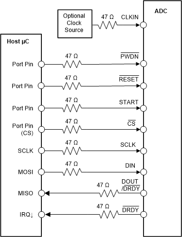
ADS1260-Q1 ADS1261-Q1 ai_serial_interface_sbas760.gifFigure 59. Serial Interface and Digital I/O Connections