JAJSF13C March   2018  – January 2019 ADS1260 , ADS1261

PRODUCTION DATA.  

  1. 特長
  2. アプリケーション
  3. 概要
    1.     Device Images
      1.      ブロック図
  4. 改訂履歴
  5. 概要(続き)
  6. Device Comparison Table
  7. Pin Configuration and Functions
    1.     Pin Functions
  8. Specifications
    1. 8.1 Absolute Maximum Ratings
    2. 8.2 ESD Ratings
    3. 8.3 Recommended Operating Conditions
    4. 8.4 Thermal Information
    5. 8.5 Electrical Characteristics
    6. 8.6 Timing Requirements
    7. 8.7 Switching Characteristics
    8. 8.8 Typical Characteristics
  9. Parameter Measurement Information
    1. 9.1 Noise Performance
  10. 10Detailed Description
    1. 10.1 Overview
    2. 10.2 Functional Block Diagram
    3. 10.3 Feature Description
      1. 10.3.1  Analog Inputs
        1. 10.3.1.1 ESD Diodes
        2. 10.3.1.2 Input Multiplexer
        3. 10.3.1.3 Temperature Sensor
        4. 10.3.1.4 Power-Supply Readback
        5. 10.3.1.5 Inputs Open
        6. 10.3.1.6 Internal VCOM Connection
        7. 10.3.1.7 Alternate Functions
      2. 10.3.2  PGA
        1. 10.3.2.1 PGA Bypass Mode
        2. 10.3.2.2 PGA Voltage Monitor
      3. 10.3.3  Reference Voltage
        1. 10.3.3.1 Internal Reference
        2. 10.3.3.2 External Reference
        3. 10.3.3.3 AVDD - AVSS Reference (Default)
        4. 10.3.3.4 Reference Monitor
      4. 10.3.4  Level-Shift Voltage (VBIAS)
      5. 10.3.5  Burn-Out Current Sources
      6. 10.3.6  Sensor-Excitation Current Sources (IDAC1 and IDAC2)
      7. 10.3.7  General-Purpose Input/Outputs (GPIOs)
      8. 10.3.8  Oversampling
      9. 10.3.9  Modulator
      10. 10.3.10 Digital Filter
        1. 10.3.10.1 Sinc Filter
          1. 10.3.10.1.1 Sinc Filter Frequency Response
        2. 10.3.10.2 FIR Filter
          1. 10.3.10.2.1 FIR Filter Frequency Response
        3. 10.3.10.3 Filter Bandwidth
        4. 10.3.10.4 50-Hz and 60-Hz Normal Mode Rejection
    4. 10.4 Device Functional Modes
      1. 10.4.1 Conversion Control
        1. 10.4.1.1 Continuous-Conversion Mode
        2. 10.4.1.2 Pulse-Conversion Mode
        3. 10.4.1.3 Conversion Latency
        4. 10.4.1.4 Start-Conversion Delay
      2. 10.4.2 Chop Mode
      3. 10.4.3 AC-Excitation Mode
      4. 10.4.4 ADC Clock Mode
      5. 10.4.5 Power-Down Mode
        1. 10.4.5.1 Hardware Power-Down
        2. 10.4.5.2 Software Power-Down
      6. 10.4.6 Reset
        1. 10.4.6.1 Power-on Reset
        2. 10.4.6.2 Reset by Pin
        3. 10.4.6.3 Reset by Command
      7. 10.4.7 Calibration
        1. 10.4.7.1 Offset and Full-Scale Calibration
          1. 10.4.7.1.1 Offset Calibration Registers
          2. 10.4.7.1.2 Full-Scale Calibration Registers
        2. 10.4.7.2 Offset Self-Calibration (SFOCAL)
        3. 10.4.7.3 Offset System-Calibration (SYOCAL)
        4. 10.4.7.4 Full-Scale Calibration (GANCAL)
        5. 10.4.7.5 Calibration Command Procedure
        6. 10.4.7.6 User Calibration Procedure
    5. 10.5 Programming
      1. 10.5.1 Serial Interface
        1. 10.5.1.1 Chip Select (CS)
        2. 10.5.1.2 Serial Clock (SCLK)
        3. 10.5.1.3 Data Input (DIN)
        4. 10.5.1.4 Data Output/Data Ready (DOUT/DRDY)
        5. 10.5.1.5 Serial Interface Auto-Reset
      2. 10.5.2 Data Ready (DRDY)
        1. 10.5.2.1 DRDY in Continuous-Conversion Mode
        2. 10.5.2.2 DRDY in Pulse-Conversion Mode
        3. 10.5.2.3 Data Ready by Software Polling
      3. 10.5.3 Conversion Data
        1. 10.5.3.1 Status byte (STATUS)
        2. 10.5.3.2 Conversion Data Format
      4. 10.5.4 CRC
      5. 10.5.5 Commands
        1. 10.5.5.1  NOP Command
        2. 10.5.5.2  RESET Command
        3. 10.5.5.3  START Command
        4. 10.5.5.4  STOP Command
        5. 10.5.5.5  RDATA Command
        6. 10.5.5.6  SYOCAL Command
        7. 10.5.5.7  GANCAL Command
        8. 10.5.5.8  SFOCAL Command
        9. 10.5.5.9  RREG Command
        10. 10.5.5.10 WREG Command
        11. 10.5.5.11 LOCK Command
        12. 10.5.5.12 UNLOCK Command
    6. 10.6 Register Map
      1. 10.6.1  Device Identification (ID) Register (address = 00h) [reset = xxh]
        1. Table 30. ID Register Field Descriptions
      2. 10.6.2  Device Status (STATUS) Register (address = 01h) [reset = 01h]
        1. Table 31. STATUS Register Field Descriptions
      3. 10.6.3  Mode 0 (MODE0) Register (address = 02h) [reset = 24h]
        1. Table 32. MODE0 Register Field Descriptions
      4. 10.6.4  Mode 1 (MODE1) Register (address = 03h) [reset = 01h]
        1. Table 33. MODE1 Register Field Descriptions
      5. 10.6.5  Mode 2 (MODE2) Register (address = 04h) [reset = 00h]
        1. Table 34. MODE2 Register Field Descriptions
      6. 10.6.6  Mode 3 (MODE3) Register (address = 05h) [reset = 00h]
        1. Table 35. MODE3 Register Field Descriptions
      7. 10.6.7  Reference Configuration (REF) Register (address = 06h) [reset = 05h]
        1. Table 36. REF Register Field Descriptions
      8. 10.6.8  Offset Calibration (OFCALx) Registers (address = 07h, 08h, 09h) [reset = 00h, 00h, 00h]
        1. Table 37. OFCAL0, OFCAL1, OFCAL2 Registers Field Description
      9. 10.6.9  Full-Scale Calibration (FSCALx) Registers (address = 0Ah, 0Bh, 0Ch) [reset = 00h, 00h, 40h]
        1. Table 38. FSCAL0, FSCAL1, FSCAL2 Registers Field Description
      10. 10.6.10 IDAC Multiplexer (IMUX) Register (address = 0Dh) [reset = FFh]
        1. Table 39. IMUX Register Field Descriptions
      11. 10.6.11 IDAC Magnitude (IMAG) Register (address = 0Eh) [reset = 00h]
        1. Table 40. IMAG Register Field Descriptions
      12. 10.6.12 Reserved (RESERVED) Register (address = 0Fh) [reset = 00h]
        1. Table 41. RESERVED Register Field Descriptions
      13. 10.6.13 PGA Configuration (PGA) Register (address = 10h) [reset = 00h]
        1. Table 42. PGA Register Field Descriptions
      14. 10.6.14 Input Multiplexer (INPMUX) Register (address = 11h) [reset = FFh]
        1. Table 43. INPMUX Register Field Descriptions
      15. 10.6.15 Input Bias (INPBIAS) Register (address = 12h) [reset = 00h]
        1. Table 44. INPBIAS Register Field Descriptions
  11. 11Application and Implementation
    1. 11.1 Application Information
      1. 11.1.1 Input Range
      2. 11.1.2 Input Overload
      3. 11.1.3 Burn-Out Current Source
      4. 11.1.4 Unused Inputs and Outputs
      5. 11.1.5 AC-Excitation
      6. 11.1.6 Serial Interface and Digital Connections
    2. 11.2 Typical Application
      1. 11.2.1 Design Requirements
      2. 11.2.2 Detailed Design Procedure
      3. 11.2.3 Application Curves
    3. 11.3 Initialization Setup
  12. 12Power Supply Recommendations
    1. 12.1 Power-Supply Decoupling
    2. 12.2 Analog Power-Supply Clamp
    3. 12.3 Power-Supply Sequencing
  13. 13Layout
    1. 13.1 Layout Guidelines
    2. 13.2 Layout Example
  14. 14デバイスおよびドキュメントのサポート
    1. 14.1 ドキュメントのサポート
      1. 14.1.1 関連資料
    2. 14.2 関連リンク
    3. 14.3 ドキュメントの更新通知を受け取る方法
    4. 14.4 コミュニティ・リソース
    5. 14.5 商標
    6. 14.6 静電気放電に関する注意事項
    7. 14.7 Glossary
  15. 15メカニカル、パッケージ、および注文情報

パッケージ・オプション

デバイスごとのパッケージ図は、PDF版データシートをご参照ください。

メカニカル・データ(パッケージ|ピン)
  • RHB|32
サーマルパッド・メカニカル・データ
発注情報

PGA

The PGA is a low-noise, CMOS differential-input, differential-output amplifier. The PGA extends the dynamic range of the ADC, important when used with low level sensors. The PGA provides gains of 1 through 32 and the ADC provides additional gains of 2 and 4. The combined gains are 1 through 128. Gain is controlled by the GAIN[2:0] register bits as shown in Figure 49. In PGA bypass mode, the input voltage range extends to the analog supplies. The PGA is powered down in bypass mode.
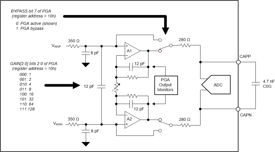
ADS1260 ADS1261 ai_pga_bd_sbas760.gifFigure 49. PGA Block Diagram

The PGA consists of two chopper-stabilized amplifiers (A1 and A2), and a resistor network that determines the PGA gain. The resistor network is precision matched, providing low drift performance. The PGA integrates noise filters to reduce sensitivity to electromagnetic-interference (EMI). The PGA output is monitored to indicate when the operating headroom is exceeded.

Pins CAPP and CAPN are the PGA positive and negative outputs, respectively. Connect an external 4.7-nF capacitor (type C0G) as shown in Figure 49. The capacitor filters the modulator sample pulses and with the internal resistors, forms the antialias filter. Place the capacitor as close as possible to the pins using short traces. Avoid running clock traces or other digital traces close to these pins.

The full-scale differential input voltage range of the ADC is determined by the reference voltage and gain. Table 4 shows the differential input voltage range verses gain for VREF = 2.5 V.

Table 4. Full-Scale Voltage Range

GAIN[2:0] BITS GAIN FULL-SCALE DIFFERENTIAL INPUT RANGE(1)
000 1 ±2.500 V
001 2 ±1.250 V
010 4 ±0.625 V
011 8 ±0.312 V
100 16 ±0.156 V
101 32 ±0.078 V
110 64 ±0.039 V
111 128 ±0.0195 V
VREF = 2.5 V. Full scale differential input voltage range is proportional to VREF.

As with many amplifiers, the PGA has an input voltage range limitation that must not be exceeded in order to maintain linear operation. The specified input voltage range is expressed as the absolute voltage at the positive and negative inputs. As specified in Equation 5, the specified absolute input voltage depends on gain, the expected maximum differential voltage, and the minimum analog power-supply voltage.

Equation 5. AVSS + 0.3 V + VIN · (Gain – 1) / 2 · < VAINP and VAINN < AVDD – 0.3 V – VIN · (Gain – 1) / 2

where

  • VAINP, VAINN = absolute input voltage
  • VIN = maximum differential input voltage = VAINP - VAINN
  • Gain (for gains = 64 and 128, use gain = 32 in the calculation)
  • AVDD = minimum AVDD voltage
  • AVSS = maximum AVSS voltage

The relationship of the PGA input to the PGA output is shown graphically in Figure 50. The PGA output voltages (VOUTP, VOUTN) depend on the respective absolute input voltage, the differential input voltage, and the PGA gain. To maintain the PGA within the linear operating range, the PGA output voltages must not exceed either AVDD – 0.3 V or AVSS + 0.3 V. The diagram depicts a positive differential input voltage that results in a positive differential output voltage.
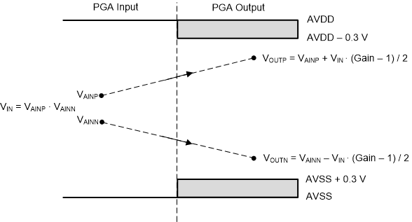
ADS1260 ADS1261 ai_pga_io_sbas760.gifFigure 50. PGA Input/Output Range