JAJSOX0A March 2024 – June 2024 ADS127L18
ADVANCE INFORMATION
- 1
- 1 特長
- 2 アプリケーション
- 3 概要
- 4 Pin Configuration and Functions
- 5 Specifications
-
6 Parameter Measurement Information
- 6.1 Offset Error Measurement
- 6.2 Offset Drift Measurement
- 6.3 Gain Error Measurement
- 6.4 Gain Drift Measurement
- 6.5 NMRR Measurement
- 6.6 CMRR Measurement
- 6.7 PSRR Measurement
- 6.8 SNR Measurement
- 6.9 INL Error Measurement
- 6.10 THD Measurement
- 6.11 IMD Measurement
- 6.12 SFDR Measurement
- 6.13 Noise Performance
-
7 Detailed Description
- 7.1 Overview
- 7.2 Functional Block Diagram
- 7.3 Feature Description
- 7.4 Device Functional Modes
- 7.5 Programming
- 8 Register Map
- 9 Application and Implementation
- 10Device and Documentation Support
- 11Revision History
- 12Mechanical, Packaging, and Orderable Information
7.3.8.1 Wideband Filter
The wideband filter is a multistage FIR design featuring linear phase response, low pass-band ripple, narrow transition band, and high stop-band attenuation. Because of these characteristics, the filter is designed for measuring ac and dc signals. The ADC provides eight programmable values of OSR and four speed modes, offering a range of data rate, resolution and data rate options.
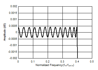
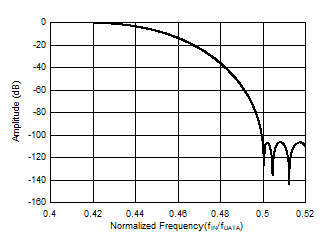
Figure 7-12 through Figure 7-16 illustrate the frequency response of the wideband filter. Figure 7-12 shows the pass-band ripple. Figure 7-13 shows the detailed frequency response at the transition band.


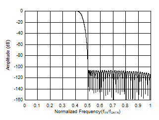
Figure 7-14 shows the frequency response to fDATA for OSR ≥ 64. The stop band begins at fDATA / 2 to prevent aliasing at the Nyquist frequency. Figure 7-15 shows the stop-band attenuation to fMOD for OSR = 32. In the stop-band region, out-of-band input frequencies mix with multiples of the fMOD / 32 chop frequency. This process creates a pattern of stop-band response peaks that exceed the attenuation provided by the digital filter. The width of the response peaks is twice the filter bandwidth. Stop-band attenuation is improved when used in conjunction with an antialias filter at the ADC input.

| OSR ≥ 64 |

| OSR = 32 |
Figure 7-16 shows the filter response centered at fMOD, where the filter response repeats. If not removed by an antialiasing filter, input frequencies at fMOD appear as aliased frequencies in the pass band. Aliasing also occurs by input frequencies occurring at multiples of fMOD. These frequency bands are defined by:
where:
- N = 1, 2, 3, and so on
- fMOD = Modulator sampling frequency
- fBW = Filter bandwidth

The group delay of the filter is the time for a signal to propagate from the input to the output of the filter. Because the filter is a linear-phase design, the envelope of a multifrequency complex signal is undistorted by filter processing. The group delay (expressed in units of time) is constant versus signal frequency and is equal to 34 / fDATA. Be aware that after a step input is applied to the ADC inputs, fully settled data occurs 68 data periods later. Figure 7-17 shows the filter group delay (34 / fDATA) and the settling time for a step input (68 / fDATA).

The digital filter is restarted when the ADC is synchronized. After synchronization, the ADC either discards 68 conversion results to account for filter settling, or immediately outputs unsettled data. The DP_MODE bit the DP_CFG1 register selects the option used. In settled-data mode, there is no need to discard data. The Latency Time column of Table 7-9 lists the time for the first data to appear. If a step input occurs asynchronous to the conversion period, then the next 69 conversions are partially settled data.
| MODE | fCLK (MHz) |
OSR | DATA RATE (kSPS) |
–0.1dB FREQUENCY (kHz) |
–3dB FREQUENCY (kHz) |
LATENCY TIME1 (µs) |
|---|---|---|---|---|---|---|
| Max speed | 32.768 | 32 | 512 | 211.2 | 223.9 | 133.2 |
| High speed | 25.6 | 400 | 165 | 174.96 | 170.6 | |
| Mid speed | 12.8 | 200 | 82.5 | 87.48 | 341.2 | |
| Low speed | 3.2 | 50 | 20.63 | 21.87 | 1364.8 | |
| Max speed | 32.768 | 64 | 256 | 105.6 | 112.0 | 266.0 |
| High speed | 25.6 | 200 | 82.5 | 87.48 | 340.6 | |
| Mid speed | 12.8 | 100 | 41.25 | 43.74 | 681.2 | |
| Low speed | 3.2 | 25 | 10.31 | 10.94 | 2724.8 | |
| Max speed | 32.768 | 128 | 128 | 52.8 | 55.99 | 531.6 |
| High speed | 25.6 | 100 | 41.25 | 43.74 | 680.6 | |
| Mid speed | 12.8 | 50 | 20.63 | 21.87 | 1361.2 | |
| Low speed | 3.2 | 12.5 | 5.1562 | 5.468 | 5444.8 | |
| Max speed | 32.768 | 256 | 64 | 26.4 | 28.00 | 1062.87 |
| High speed | 25.6 | 50 | 20.625 | 21.87 | 1360.6 | |
| Mid speed | 12.8 | 25 | 10.31 | 10.93 | 2721.2 | |
| Low speed | 3.2 | 6.25 | 2.578 | 2.734 | 10884.8 | |
| Max speed | 32.768 | 512 | 32 | 13.2 | 14.00 | 2125.37 |
| High speed | 25.6 | 25 | 10.312 | 10.935 | 2720.6 | |
| Mid speed | 12.8 | 12.5 | 5.156 | 5.467 | 5441.2 | |
| Low speed | 3.2 | 3.125 | 1.289 | 1.367 | 21764.8 | |
| Max speed | 32.768 | 1024 | 16 | 6.6 | 7.998 | 4250.4 |
| High speed | 25.6 | 12.5 | 5.156 | 5.467 | 5440.6 | |
| Mid speed | 12.8 | 6.25 | 2.578 | 2.734 | 10881.2 | |
| Low speed | 3.2 | 1.5625 | 0.645 | 0.6834 | 43524.8 | |
| Max speed | 32.768 | 2048 | 8 | 3.3 | 3.499 | 8500.4 |
| High speed | 25.6 | 6.25 | 2.578 | 2.734 | 10880.6 | |
| Mid speed | 12.8 | 3.125 | 1.289 | 1.367 | 21761.2 | |
| Low speed | 3.2 | 0.78125 | 0.322 | 0.3417 | 87044.8 | |
| Max speed | 32.768 | 4096 | 4 | 1.65 | 1.750 | 17000.4 |
| High speed | 25.6 | 3.125 | 1.289 | 1.367 | 21760.6 | |
| Mid speed | 12.8 | 1.5625 | 0.645 | 0.6834 | 43521.1 | |
| Low speed | 3.2 | 0.390625 | 0.161 | 0.1709 | 174084.8 |