JAJSHV4C January 2014 – August 2019 ADS1283
PRODUCTION DATA.
- 1 特長
- 2 アプリケーション
- 3 概要
- 4 改訂履歴
- 5 Pin Configuration and Functions
- 6 Specifications
- 7 Parameter Measurement Information
-
8 Detailed Description
- 8.1 Overview
- 8.2 Functional Block Diagram
- 8.3 Feature Description
- 8.4
Device Functional Modes
- 8.4.1 Synchronization (SYNC PIN and SYNC Command)
- 8.4.2 Reset (RESET Pin and Reset Command)
- 8.4.3 Power-Down (PWDN Pin and STANDBY Command)
- 8.4.4 Power-On Sequence
- 8.4.5 DVDD Power Supply
- 8.4.6 Serial Interface
- 8.4.7 Data Format
- 8.4.8 Reading Data
- 8.4.9 One-Shot Operation
- 8.4.10 Offset and Full-Scale Calibration Registers
- 8.4.11 Calibration Commands (OFSCAL and GANCAL)
- 8.4.12 User Calibration
- 8.5
Programming
- 8.5.1
Commands
- 8.5.1.1 SDATAC Requirements
- 8.5.1.2 WAKEUP: Wake-Up From Standby Mode
- 8.5.1.3 STANDBY: Standby Mode
- 8.5.1.4 SYNC: Synchronize the Analog-to-Digital Conversion
- 8.5.1.5 RESET: Reset the Device
- 8.5.1.6 RDATAC: Read Data Continuous
- 8.5.1.7 SDATAC: Stop Read Data Continuous
- 8.5.1.8 RDATA: Read Data by Command
- 8.5.1.9 RREG: Read Register Data
- 8.5.1.10 WREG: Write to Register
- 8.5.1.11 OFSCAL: Offset Calibration
- 8.5.1.12 GANCAL: Gain Calibration
- 8.5.1
Commands
- 8.6
Register Maps
- 8.6.1
Register Descriptions
- 8.6.1.1 ID_CFG: ID_Configuration Register (address = 00h) [reset =x0h]
- 8.6.1.2 CONFIG0: Configuration Register 0 (address = 01h) [reset = 52h]
- 8.6.1.3 CONFIG1: Configuration Register 1 (address = 02h) [reset = 08h]
- 8.6.1.4 HPF0 and HPF1 Registers
- 8.6.1.5 OFC0, OFC1, OFC2 Registers
- 8.6.1.6 FSC0, FSC1, FSC2 Registers
- 8.6.1
Register Descriptions
- 9 Application and Implementation
- 10デバイスおよびドキュメントのサポート
- 11メカニカル、パッケージ、および注文情報
8.3.1 Analog Inputs and Multiplexer
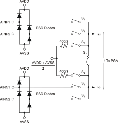
A diagram of the input multiplexer is shown in Figure 25.
 Figure 25. Analog Inputs and Multiplexer
 ESD diodes protect the multiplexer inputs. If either input is taken below AVSS – 0.3 V, or above AVDD + 0.3 V, the ESD protection diodes can turn on. If these conditions are possible, use external clamp diodes, series resistors, or both to limit the input current to safe values (see the Absolute Maximum Ratings table).
Also, overdriving one unused input can affect the conversions of the other input. If an overdriven input interacts with the measured input, clamp the overdriven signal with external Schottky diodes.
The specified input operating range of the PGA is shown in Equation 2:

For best operation, maintain absolute input levels (input signal level and common-mode level) within these limits.
The multiplexer connects one of the two external differential inputs to the preamplifier inputs, in addition to internal connections for various self-test modes. Table 3 summarizes the multiplexer configurations for Figure 25.
Table 3. Multiplexer Modes
| MUX[2:0] | SWITCHES | DESCRIPTION |
|---|---|---|
| 000 | S1, S5 | AINP1 and AINN1 connected to preamplifier |
| 001 | S2, S6 | AINP2 and AINN2 connected to preamplifier |
| 010 | S3, S4 | Preamplifier inputs shorted together through 400-Ω internal resistors |
| 011 | S1, S5, S2, S6 | AINP1, AINN1 and AINP2, AINN2 connected together and to the preamplifier |
| 100 | S6, S7 | External short, preamplifier inputs shorted to AINN2 (common-mode test) |
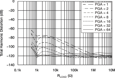
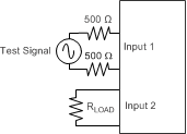
The typical on-resistance (RON) of the multiplexer is 30 Ω (each switch). When the multiplexer is used to drive an external load on one input by a signal generator on the other input, on-resistance and on-resistance amplitude dependency can lead to measurement errors. Figure 26 shows THD versus load resistance and amplitude. THD improves with high-impedance loads and with lower-amplitude drive signals. The data are measured with the circuit from Figure 27 with MUX[2:0] = 011.
 Figure 26. THD vs External Load and Signal Magnitude (PGA); See Figure 27
  Figure 27. Driving an External Load Through the Multiplexer