JAJSHV4C January 2014 – August 2019 ADS1283
PRODUCTION DATA.
- 1 特長
- 2 アプリケーション
- 3 概要
- 4 改訂履歴
- 5 Pin Configuration and Functions
- 6 Specifications
- 7 Parameter Measurement Information
-
8 Detailed Description
- 8.1 Overview
- 8.2 Functional Block Diagram
- 8.3 Feature Description
- 8.4
Device Functional Modes
- 8.4.1 Synchronization (SYNC PIN and SYNC Command)
- 8.4.2 Reset (RESET Pin and Reset Command)
- 8.4.3 Power-Down (PWDN Pin and STANDBY Command)
- 8.4.4 Power-On Sequence
- 8.4.5 DVDD Power Supply
- 8.4.6 Serial Interface
- 8.4.7 Data Format
- 8.4.8 Reading Data
- 8.4.9 One-Shot Operation
- 8.4.10 Offset and Full-Scale Calibration Registers
- 8.4.11 Calibration Commands (OFSCAL and GANCAL)
- 8.4.12 User Calibration
- 8.5
Programming
- 8.5.1
Commands
- 8.5.1.1 SDATAC Requirements
- 8.5.1.2 WAKEUP: Wake-Up From Standby Mode
- 8.5.1.3 STANDBY: Standby Mode
- 8.5.1.4 SYNC: Synchronize the Analog-to-Digital Conversion
- 8.5.1.5 RESET: Reset the Device
- 8.5.1.6 RDATAC: Read Data Continuous
- 8.5.1.7 SDATAC: Stop Read Data Continuous
- 8.5.1.8 RDATA: Read Data by Command
- 8.5.1.9 RREG: Read Register Data
- 8.5.1.10 WREG: Write to Register
- 8.5.1.11 OFSCAL: Offset Calibration
- 8.5.1.12 GANCAL: Gain Calibration
- 8.5.1
Commands
- 8.6
Register Maps
- 8.6.1
Register Descriptions
- 8.6.1.1 ID_CFG: ID_Configuration Register (address = 00h) [reset =x0h]
- 8.6.1.2 CONFIG0: Configuration Register 0 (address = 01h) [reset = 52h]
- 8.6.1.3 CONFIG1: Configuration Register 1 (address = 02h) [reset = 08h]
- 8.6.1.4 HPF0 and HPF1 Registers
- 8.6.1.5 OFC0, OFC1, OFC2 Registers
- 8.6.1.6 FSC0, FSC1, FSC2 Registers
- 8.6.1
Register Descriptions
- 9 Application and Implementation
- 10デバイスおよびドキュメントのサポート
- 11メカニカル、パッケージ、および注文情報
8.3.2 Programmable Gain Amplifier (PGA)
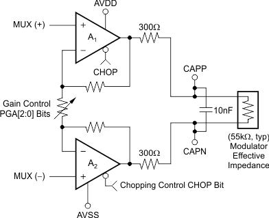
The PGA of the ADS1283 is a low-noise, continuous-time, differential-in and differential-out CMOS amplifier. The gain is set by register bits PGA[2:0], and is programmable from 1 to 64 for the ADS1283, or can be set to 1, 4, and 16 for the ADS1283A. The PGA differentially drives the modulator through 300-Ω internal resistors. A C0G capacitor (10-nF C0G or film dielectric) must be connected to CAPP and CAPN to filter modulator sampling glitches. The external capacitor also serves as an antialias filter. The corner frequency is given in Equation 3:

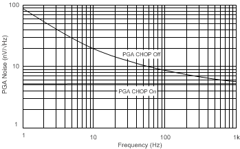
The ADS1283 PGA provides a chop feature. As shown in Figure 28, amplifiers A1 and A2 are chopper stabilized to remove the offset, offset drift, and 1/f noise. Chopper stabilization (or chopping) moves the offset and noise to fCLK / 1024 (4 kHz, fCLK = 4.096 MHz ), which is located safely out of the pass-band frequency. Chopping can be disabled by setting the CHOP bit = 0. When chopping is disabled, the PGA input impedance increases (see Differential Input Impedance parameter in the Electrical Characteristics). As shown in Figure 29, chopping maintains flat noise density, leaving predominantly white noise. However, if chopping is disabled, the PGA input noise results in a rising 1/f noise profile.

 Figure 29. PGA Noise
 As a result of the stray capacitance of the input chopping switches, low-level transient currents flow through the inputs when chopping is enabled. The average value of the transient currents versus the input voltage results in an effective input impedance. The effective input impedance depends on the PGA gain, as shown in Table 4. Despite the relatively high input impedance, carefully evaluate applications with high-impedance sensors or high-impedance termination resistors when chopping is enabled. Table 4 shows the PGA differential input impedance with CHOP enabled.
Table 4. Differential Input Impedance (CHOP Enabled)
| PGA | DIFFERENTIAL INPUT IMPEDANCE (GΩ) |
|---|---|
| 1 | 7 |
| 2 | 7 |
| 4 | 4 |
| 8 | 3 |
| 16 | 2 |
| 32 | 1 |
| 64 | 0.5 |
The PGA has programmable gains from 1 to 64. Table 5 shows the register bit setting for the PGA and resulting full-scale differential range.
Table 5. PGA Gain Settings
| PGA[2:0] | GAIN(2) | DIFFERENTIAL INPUT RANGE (V)(1) |
|---|---|---|
| 000 | 1 | ±2.5 |
| 001 | 2 | ±1.25 |
| 010 | 4 | ±0.625 |
| 011 | 8 | ±0.312 |
| 100 | 16 | ±0.156 |
| 101 | 32 | ±0.078 |
| 110 | 64 | ±0.039 |
The specified range of the PGA output is shown in Equation 4:

For best performance, maintain PGA output levels (signal + common-mode) within these limits.