JAJSHV4C January 2014 – August 2019 ADS1283
PRODUCTION DATA.
- 1 特長
- 2 アプリケーション
- 3 概要
- 4 改訂履歴
- 5 Pin Configuration and Functions
- 6 Specifications
- 7 Parameter Measurement Information
-
8 Detailed Description
- 8.1 Overview
- 8.2 Functional Block Diagram
- 8.3 Feature Description
- 8.4
Device Functional Modes
- 8.4.1 Synchronization (SYNC PIN and SYNC Command)
- 8.4.2 Reset (RESET Pin and Reset Command)
- 8.4.3 Power-Down (PWDN Pin and STANDBY Command)
- 8.4.4 Power-On Sequence
- 8.4.5 DVDD Power Supply
- 8.4.6 Serial Interface
- 8.4.7 Data Format
- 8.4.8 Reading Data
- 8.4.9 One-Shot Operation
- 8.4.10 Offset and Full-Scale Calibration Registers
- 8.4.11 Calibration Commands (OFSCAL and GANCAL)
- 8.4.12 User Calibration
- 8.5
Programming
- 8.5.1
Commands
- 8.5.1.1 SDATAC Requirements
- 8.5.1.2 WAKEUP: Wake-Up From Standby Mode
- 8.5.1.3 STANDBY: Standby Mode
- 8.5.1.4 SYNC: Synchronize the Analog-to-Digital Conversion
- 8.5.1.5 RESET: Reset the Device
- 8.5.1.6 RDATAC: Read Data Continuous
- 8.5.1.7 SDATAC: Stop Read Data Continuous
- 8.5.1.8 RDATA: Read Data by Command
- 8.5.1.9 RREG: Read Register Data
- 8.5.1.10 WREG: Write to Register
- 8.5.1.11 OFSCAL: Offset Calibration
- 8.5.1.12 GANCAL: Gain Calibration
- 8.5.1
Commands
- 8.6
Register Maps
- 8.6.1
Register Descriptions
- 8.6.1.1 ID_CFG: ID_Configuration Register (address = 00h) [reset =x0h]
- 8.6.1.2 CONFIG0: Configuration Register 0 (address = 01h) [reset = 52h]
- 8.6.1.3 CONFIG1: Configuration Register 1 (address = 02h) [reset = 08h]
- 8.6.1.4 HPF0 and HPF1 Registers
- 8.6.1.5 OFC0, OFC1, OFC2 Registers
- 8.6.1.6 FSC0, FSC1, FSC2 Registers
- 8.6.1
Register Descriptions
- 9 Application and Implementation
- 10デバイスおよびドキュメントのサポート
- 11メカニカル、パッケージ、および注文情報
8.3.3.1.5 Voltage Reference Inputs (VREFP, VREFN)
The voltage reference for the ADS1283 is the differential voltage between VREFP and VREFN:
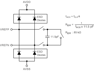
The reference inputs use a structure similar to that of the analog inputs with the circuitry of the reference inputs shown in Figure 34. The average load presented by the switched-capacitor reference input can be modeled with an effective differential impedance of:
Note that the effective impedance of the reference inputs loads the external reference.
 Figure 34. Simplified Reference Input Circuit
 Place a 0.1-µF ceramic capacitor directly between the ADC VREFP and VREFN pins. Multiple ADC applications can share a single voltage reference, but must have individual capacitors placed for each ADC.
The ADS1283 reference inputs are protected by ESD diodes. In order to prevent these diodes from turning on, the voltage on either input must stay within the range shown in Equation 8:

The minimum valid input for VREFN is AVSS – 0.1 V, and the maximum valid input for VREFP is AVDD + 0.1 V.
To achieve the best performance from the ADS1283, use a high-quality 5-V reference voltage. A 4-V or 4.5-V reference voltage can be used; however, this lower reference voltage reduces the signal input range with a corresponding decrease of SNR. Noise and drift on the reference degrade overall system performance. To achieve optimum performance, make sure to give special care to the circuitry generating the reference voltages. See the Application Information section for reference recommendations.