JAJSHV4C January   2014  – August 2019 ADS1283

PRODUCTION DATA.  

  1. 特長
  2. アプリケーション
    1.     概略回路図
  3. 概要
  4. 改訂履歴
  5. Pin Configuration and Functions
    1.     Pin Functions
  6. Specifications
    1. 6.1 Absolute Maximum Ratings
    2. 6.2 ESD Ratings
    3. 6.3 Recommended Operating Conditions
    4. 6.4 Thermal Information
    5. 6.5 Electrical Characteristics
    6. 6.6 Timing Requirements
    7. 6.7 Switching Characteristics
    8. 6.8 Typical Characteristics
  7. Parameter Measurement Information
    1. 7.1 Noise Performance
  8. Detailed Description
    1. 8.1 Overview
    2. 8.2 Functional Block Diagram
    3. 8.3 Feature Description
      1. 8.3.1 Analog Inputs and Multiplexer
      2. 8.3.2 Programmable Gain Amplifier (PGA)
      3. 8.3.3 Analog-to-Digital Converter (ADC)
        1. 8.3.3.1 Modulator
          1. 8.3.3.1.1 Modulator Overrange
          2. 8.3.3.1.2 Modulator Input Impedance
          3. 8.3.3.1.3 Modulator Overrange Detection (MFLAG)
          4. 8.3.3.1.4 Offset
          5. 8.3.3.1.5 Voltage Reference Inputs (VREFP, VREFN)
        2. 8.3.3.2 Digital Filter
          1. 8.3.3.2.1 Sinc Filter Stage (sinx / x)
          2. 8.3.3.2.2 FIR Stage
          3. 8.3.3.2.3 Group Delay and Step Response
            1. 8.3.3.2.3.1 Linear Phase Response
            2. 8.3.3.2.3.2 Minimum Phase Response
          4. 8.3.3.2.4 HPF Stage
      4. 8.3.4 Master Clock Input (CLK)
    4. 8.4 Device Functional Modes
      1. 8.4.1  Synchronization (SYNC PIN and SYNC Command)
        1. 8.4.1.1 Pulse-Sync Mode
        2. 8.4.1.2 Continuous-Sync Mode
      2. 8.4.2  Reset (RESET Pin and Reset Command)
      3. 8.4.3  Power-Down (PWDN Pin and STANDBY Command)
      4. 8.4.4  Power-On Sequence
      5. 8.4.5  DVDD Power Supply
      6. 8.4.6  Serial Interface
        1. 8.4.6.1 Chip Select (CS)
        2. 8.4.6.2 Serial Clock (SCLK)
        3. 8.4.6.3 Data Input (DIN)
        4. 8.4.6.4 Data Output (DOUT)
        5. 8.4.6.5 Serial Port Auto Timeout
        6. 8.4.6.6 Data Ready (DRDY)
      7. 8.4.7  Data Format
      8. 8.4.8  Reading Data
        1. 8.4.8.1 Read-Data-Continuous Mode
        2. 8.4.8.2 Read-Data-By-Command Mode
      9. 8.4.9  One-Shot Operation
      10. 8.4.10 Offset and Full-Scale Calibration Registers
        1. 8.4.10.1 OFC[2:0] Registers
        2. 8.4.10.2 FSC[2:0] Registers
      11. 8.4.11 Calibration Commands (OFSCAL and GANCAL)
        1. 8.4.11.1 OFSCAL Command
        2. 8.4.11.2 GANCAL Command
      12. 8.4.12 User Calibration
    5. 8.5 Programming
      1. 8.5.1 Commands
        1. 8.5.1.1  SDATAC Requirements
        2. 8.5.1.2  WAKEUP: Wake-Up From Standby Mode
        3. 8.5.1.3  STANDBY: Standby Mode
        4. 8.5.1.4  SYNC: Synchronize the Analog-to-Digital Conversion
        5. 8.5.1.5  RESET: Reset the Device
        6. 8.5.1.6  RDATAC: Read Data Continuous
        7. 8.5.1.7  SDATAC: Stop Read Data Continuous
        8. 8.5.1.8  RDATA: Read Data by Command
        9. 8.5.1.9  RREG: Read Register Data
        10. 8.5.1.10 WREG: Write to Register
        11. 8.5.1.11 OFSCAL: Offset Calibration
        12. 8.5.1.12 GANCAL: Gain Calibration
    6. 8.6 Register Maps
      1. 8.6.1 Register Descriptions
        1. 8.6.1.1 ID_CFG: ID_Configuration Register (address = 00h) [reset =x0h]
        2. 8.6.1.2 CONFIG0: Configuration Register 0 (address = 01h) [reset = 52h]
        3. 8.6.1.3 CONFIG1: Configuration Register 1 (address = 02h) [reset = 08h]
        4. 8.6.1.4 HPF0 and HPF1 Registers
          1. 8.6.1.4.1 HPF0: High-Pass Filter Corner Frequency, Low Byte (address = 03h) [reset = 32h]
          2. 8.6.1.4.2 HPF1: High-Pass Filter Corner Frequency, High Byte (address = 04h) [reset = 03h]
        5. 8.6.1.5 OFC0, OFC1, OFC2 Registers
          1. 8.6.1.5.1 OFC0: Offset Calibration, Low Byte (address = 05h) [reset = 00h]
          2. 8.6.1.5.2 OFC1: Offset Calibration, Mid Byte (address = 06h) [reset = 00h]
          3. 8.6.1.5.3 OFC2: Offset Calibration, High Byte (address = 07h) [reset = 00h]
        6. 8.6.1.6 FSC0, FSC1, FSC2 Registers
          1. 8.6.1.6.1 FSC0: Full-Scale Calibration, Low Byte (address = 08h) [reset = 00h]
          2. 8.6.1.6.2 FSC1: Full-Scale Calibration, Mid Byte (address = 09h) [reset = 00h]
          3. 8.6.1.6.3 FSC2: Full-Scale Calibration, High Byte (address = 0Ah) [reset = 40h]
  9. Application and Implementation
    1. 9.1 Application Information
    2. 9.2 Typical Applications
      1. 9.2.1 Geophone Interface
      2. 9.2.2 Digital Interface
    3. 9.3 Initialization Set Up
  10. 10デバイスおよびドキュメントのサポート
    1. 10.1 ドキュメントの更新通知を受け取る方法
    2. 10.2 コミュニティ・リソース
    3. 10.3 商標
    4. 10.4 静電気放電に関する注意事項
    5. 10.5 Glossary
  11. 11メカニカル、パッケージ、および注文情報

パッケージ・オプション

メカニカル・データ(パッケージ|ピン)
サーマルパッド・メカニカル・データ
発注情報

Sinc Filter Stage (sinx / x)

The sinc filter is a variable decimation rate, fifth-order, low-pass filter. Data are supplied to this section of the filter from the modulator at the rate of fMOD (fCLK / 4). The sinc filter attenuates the high-frequency noise of the modulator, then decimates the data stream into parallel data. The decimation rate affects the overall data rate of the converter, and is set by the DR[2:0] register bits, as shown in Table 7.

Table 7. Sinc Filter Data Rates

DR[2:0] REGISTER DECIMATION RATIO (N) DATA RATE (SPS)
000 128 8,000
001 64 16,000
010 32 32,000
011 16 64,000
100 8 128,000

Equation 9 shows the scaled Z-domain transfer function of the sinc filter.

Equation 9. ADS1283 q_hz_bas418.gif

where

  • N = decimation ratio

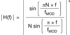
Equation 10 shows the frequency domain transfer function of the sinc filter.

Equation 10. ADS1283 q_hf_bas418.gif

where

  • N = decimation ratio (see Table 7)

The sinc filter has notches (or zeros) that occur at the output data rate and multiples thereof. At these frequencies, the filter has zero gain. Figure 36 shows the frequency response of the sinc filter and Figure 37 shows the roll-off of the sinc filter.
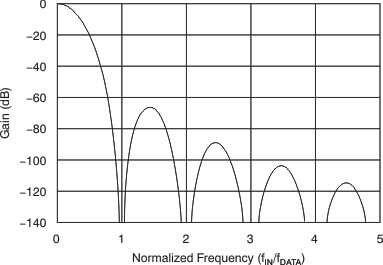
ADS1283 ai_sinc_gain-freq_bas418.gifFigure 36. Sinc Filter Frequency Response
(N = 32)
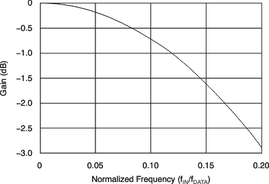
ADS1283 ai_sinc_rolloff_bas418.gifFigure 37. Sinc Filter Roll-Off