JAJSHV4C January 2014 – August 2019 ADS1283
PRODUCTION DATA.
- 1 特長
- 2 アプリケーション
- 3 概要
- 4 改訂履歴
- 5 Pin Configuration and Functions
- 6 Specifications
- 7 Parameter Measurement Information
-
8 Detailed Description
- 8.1 Overview
- 8.2 Functional Block Diagram
- 8.3 Feature Description
- 8.4
Device Functional Modes
- 8.4.1 Synchronization (SYNC PIN and SYNC Command)
- 8.4.2 Reset (RESET Pin and Reset Command)
- 8.4.3 Power-Down (PWDN Pin and STANDBY Command)
- 8.4.4 Power-On Sequence
- 8.4.5 DVDD Power Supply
- 8.4.6 Serial Interface
- 8.4.7 Data Format
- 8.4.8 Reading Data
- 8.4.9 One-Shot Operation
- 8.4.10 Offset and Full-Scale Calibration Registers
- 8.4.11 Calibration Commands (OFSCAL and GANCAL)
- 8.4.12 User Calibration
- 8.5
Programming
- 8.5.1
Commands
- 8.5.1.1 SDATAC Requirements
- 8.5.1.2 WAKEUP: Wake-Up From Standby Mode
- 8.5.1.3 STANDBY: Standby Mode
- 8.5.1.4 SYNC: Synchronize the Analog-to-Digital Conversion
- 8.5.1.5 RESET: Reset the Device
- 8.5.1.6 RDATAC: Read Data Continuous
- 8.5.1.7 SDATAC: Stop Read Data Continuous
- 8.5.1.8 RDATA: Read Data by Command
- 8.5.1.9 RREG: Read Register Data
- 8.5.1.10 WREG: Write to Register
- 8.5.1.11 OFSCAL: Offset Calibration
- 8.5.1.12 GANCAL: Gain Calibration
- 8.5.1
Commands
- 8.6
Register Maps
- 8.6.1
Register Descriptions
- 8.6.1.1 ID_CFG: ID_Configuration Register (address = 00h) [reset =x0h]
- 8.6.1.2 CONFIG0: Configuration Register 0 (address = 01h) [reset = 52h]
- 8.6.1.3 CONFIG1: Configuration Register 1 (address = 02h) [reset = 08h]
- 8.6.1.4 HPF0 and HPF1 Registers
- 8.6.1.5 OFC0, OFC1, OFC2 Registers
- 8.6.1.6 FSC0, FSC1, FSC2 Registers
- 8.6.1
Register Descriptions
- 9 Application and Implementation
- 10デバイスおよびドキュメントのサポート
- 11メカニカル、パッケージ、および注文情報
8.3.3.2.4 HPF Stage
The last stage of the ADS1283 filter block is a first-order HPF implemented as an IIR structure. This filter stage blocks dc signals, and rolls off low-frequency components below the cutoff frequency. The transfer function for the filter is shown in Equation 11:

The high-pass corner frequency is programmed by registers HPF[1:0], in hexadecimal. Equation 13 is used to set the high-pass corner frequency. Table 11 lists example values for the high-pass filter.

where
- HPF = High-pass filter register value (converted to hexadecimal)
- ωN = 2πfHP / fDATA (normalized frequency, radians)
- fHP = High-pass corner frequency (Hz)
- fDATA = Data rate (Hz)
Table 11. High-Pass Filter Value Examples
| fHP (Hz) | DATA RATE (SPS) | HPF[1:0] |
|---|---|---|
| 0.5 | 250 | 0337h |
| 1.0 | 500 | 0337h |
| 1.0 | 1000 | 019Ah |
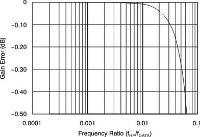
The HPF causes a small gain error, in which case the magnitude of the error depends on the ratio of fHP / fDATA. For many common values of (fHP / fDATA), the gain error is negligible. Figure 43 shows the gain error of the HPF.
 Figure 43. HPF Gain Error
 The gain error factor is illustrated in Equation 14:

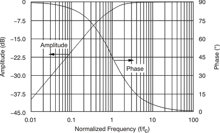
Figure 44 shows the first-order amplitude and phase response of the HPF. In the case of applying step inputs or synchronizing, make sure to take the settling time of the filter into account.
 Figure 44. HPF Amplitude and Phase Response