JAJSHV4C January 2014 – August 2019 ADS1283
PRODUCTION DATA.
- 1 特長
- 2 アプリケーション
- 3 概要
- 4 改訂履歴
- 5 Pin Configuration and Functions
- 6 Specifications
- 7 Parameter Measurement Information
-
8 Detailed Description
- 8.1 Overview
- 8.2 Functional Block Diagram
- 8.3 Feature Description
- 8.4
Device Functional Modes
- 8.4.1 Synchronization (SYNC PIN and SYNC Command)
- 8.4.2 Reset (RESET Pin and Reset Command)
- 8.4.3 Power-Down (PWDN Pin and STANDBY Command)
- 8.4.4 Power-On Sequence
- 8.4.5 DVDD Power Supply
- 8.4.6 Serial Interface
- 8.4.7 Data Format
- 8.4.8 Reading Data
- 8.4.9 One-Shot Operation
- 8.4.10 Offset and Full-Scale Calibration Registers
- 8.4.11 Calibration Commands (OFSCAL and GANCAL)
- 8.4.12 User Calibration
- 8.5
Programming
- 8.5.1
Commands
- 8.5.1.1 SDATAC Requirements
- 8.5.1.2 WAKEUP: Wake-Up From Standby Mode
- 8.5.1.3 STANDBY: Standby Mode
- 8.5.1.4 SYNC: Synchronize the Analog-to-Digital Conversion
- 8.5.1.5 RESET: Reset the Device
- 8.5.1.6 RDATAC: Read Data Continuous
- 8.5.1.7 SDATAC: Stop Read Data Continuous
- 8.5.1.8 RDATA: Read Data by Command
- 8.5.1.9 RREG: Read Register Data
- 8.5.1.10 WREG: Write to Register
- 8.5.1.11 OFSCAL: Offset Calibration
- 8.5.1.12 GANCAL: Gain Calibration
- 8.5.1
Commands
- 8.6
Register Maps
- 8.6.1
Register Descriptions
- 8.6.1.1 ID_CFG: ID_Configuration Register (address = 00h) [reset =x0h]
- 8.6.1.2 CONFIG0: Configuration Register 0 (address = 01h) [reset = 52h]
- 8.6.1.3 CONFIG1: Configuration Register 1 (address = 02h) [reset = 08h]
- 8.6.1.4 HPF0 and HPF1 Registers
- 8.6.1.5 OFC0, OFC1, OFC2 Registers
- 8.6.1.6 FSC0, FSC1, FSC2 Registers
- 8.6.1
Register Descriptions
- 9 Application and Implementation
- 10デバイスおよびドキュメントのサポート
- 11メカニカル、パッケージ、および注文情報
9.2.1 Geophone Interface
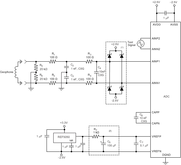
A typical geophone front-end application is shown in Figure 73. The application diagram shows the ADS1283 operation with dual ±2.5-V analog supplies. The ADS1283 can also operate with a single 5-V analog supply.

The geophone input signal is filtered by both a differential filter (components C4 and R1 to R4) and by common-mode filters (components C2, C3 and R1, R2). The differential filter removes high-frequency normal-mode components from the input signal. The common-mode filters remove high-frequency components that are common to both input leads. The input filters are not required for all applications; check the system requirements for each application.
Resistors R5 and R6 bias the signal input to the midsupply point (ground). For single-supply operation, set the bias to a low impedance midsupply point (AVDD / 2 = 2.5 V).
Optional diode clamps protect the ADS1283 inputs from high-level voltage transients and overloads. The diodes provide additional protection if possible high-level input transients and surges exceed the ADC internal ESD diode rating.
The REF5050 5-V reference provides the reference to the ADC. An optional filter network (R7 and C5) reduces the in-band reference noise for improved dynamic performance. However, the RC filter network increases the filter settling-time (from seconds to possibly minutes) depending on the dielectric absorption properties of capacitor C5. Capacitor C7 is mandatory and provides high-frequency bypassing of the reference inputs; place C7 as close as possible to the ADS1283 pins. Resistor R7 (1 kΩ) results in a 1% systematic gain error. Multiple ADCs can share a single reference, but if shared, use independent reference filters for each ADC.
As an alternative, the REF5045 (4.5 V) reference can be used. The REF5045 reference has the advantage of operating directly from the 5-V (total) power supply; however, the 4.5-V reference reduces signal range by 10% and results in a 1-dB loss of SNR.
Capacitor C6 (10 nF) filters the PGA output glitches caused by sampling of the modulator. This capacitor also forms an antialias filter with a low-pass cutoff frequency of 26 kHz.