JAJSFC6C May 2015 – April 2018 ADS52J90
PRODUCTION DATA.
- 1 特長
- 2 アプリケーション
- 3 概要
- 4 改訂履歴
- 5 概要(続き)
- 6 Pin Configuration and Functions
-
7 Specifications
- 7.1 Absolute Maximum Ratings
- 7.2 ESD Ratings
- 7.3 Recommended Operating Conditions
- 7.4 Thermal Information
- 7.5 Electrical Characteristics
- 7.6 Digital Characteristics
- 7.7 Timing Requirements: Signal Chain
- 7.8 Timing Requirements: JESD Interface
- 7.9 Timing Requirements: Serial Interface
- 7.10 Typical Characteristics
- 7.11 Typical Characteristics: JESD Interface
- 7.12 Typical Characteristics: Contour Plots
-
8 Detailed Description
- 8.1 Overview
- 8.2 Functional Block Diagrams
- 8.3
Feature Description
- 8.3.1 Connection of the External Inputs to the Input Pins
- 8.3.2 Input Multiplexer and Sampler
- 8.3.3 Analog-to-Digital Converter (ADC)
- 8.3.4 Device Synchronization Using TX_TRIG
- 8.3.5 Digital Processing
- 8.3.6 Data Formatting
- 8.3.7 Serializer and LVDS Interface
- 8.3.8 LVDS Buffers
- 8.3.9 JESD204B Interface
- 8.3.10 Interfacing SYNC~ and SYSREF Between the FPGA and ADCs
- 8.3.11 Clock Input
- 8.3.12 Analog Input and Driving Circuit
- 8.4 Device Functional Modes
- 8.5 Programming
- 9 Application and Implementation
- 10Power Supply Recommendations
- 11Layout
-
12Register Map
- 12.1
ADC Registers
- 12.1.1
Description of Registers
- 12.1.1.1 Register 0h (address = 0h)
- 12.1.1.2 Register 1h (address = 1h)
- 12.1.1.3 Register 2h (address = 2h)
- 12.1.1.4 Register 3h (address = 3h)
- 12.1.1.5 Register 4h (address = 4h)
- 12.1.1.6 Register 5h (address = 5h)
- 12.1.1.7 Register 7h (address = 7h)
- 12.1.1.8 Register 8h (address = 8h)
- 12.1.1.9 Register Ah (address = Ah)
- 12.1.1.10 Register Bh (address = Bh)
- 12.1.1.11 Register Dh (address = Dh)
- 12.1.1.12 Register Eh (address = Eh)
- 12.1.1.13 Register Fh (address = Fh)
- 12.1.1.14 Register 10h (address = 10h)
- 12.1.1.15 Register 11h (address = 11h)
- 12.1.1.16 Register 12h (address = 12h)
- 12.1.1.17 Register 13h (address = 13h)
- 12.1.1.18 Register 14h (address = 14h)
- 12.1.1.19 Register 15h (address = 15h)
- 12.1.1.20 Register 17h (address = 17h)
- 12.1.1.21 Register 18h (address = 18h)
- 12.1.1.22 Register 19h (address = 19h)
- 12.1.1.23 Register 1Ah (address = 1Ah)
- 12.1.1.24 Register 1Bh (address = 1Bh)
- 12.1.1.25 Register 1Ch (address = 1Ch)
- 12.1.1.26 Register 1Dh (address = 1Dh)
- 12.1.1.27 Register 1Eh (address = 1Eh)
- 12.1.1.28 Register 1Fh (address = 1Fh)
- 12.1.1.29 Register 20h (address = 20h)
- 12.1.1.30 Register 21h (offset = 21h)
- 12.1.1.31 Register 23h (register = 23h)
- 12.1.1.32 Register 24h (address = 24h)
- 12.1.1.33 Register 25h (address = 25h)
- 12.1.1.34 Register 26h (address = 26h)
- 12.1.1.35 Register 27h (address = 27h)
- 12.1.1.36 Register 28h (address = 28h)
- 12.1.1.37 Register 29h (address = 29h)
- 12.1.1.38 Register 2Ah (address = 2Ah)
- 12.1.1.39 Register 2Bh (address = 2Bh)
- 12.1.1.40 Register 2Ch (address = 2Ch)
- 12.1.1.41 Register 2Dh (address = 2Dh)
- 12.1.1.42 Register 2Fh (address = 2Fh)
- 12.1.1.43 Register 30h (address = 30h)
- 12.1.1.44 Register 31h (address = 31h)
- 12.1.1.45 Register 32h (address = 32h)
- 12.1.1.46 Register 33h (address = 33h)
- 12.1.1.47 Register 34h (address = 34h)
- 12.1.1.48 Register 35h (address = 35h)
- 12.1.1.49 Register 36h (address = 36h)
- 12.1.1.50 Register 37h (address = 37h)
- 12.1.1.51 Register 38h (address = 38h)
- 12.1.1.52 Register 39h (address = 39h)
- 12.1.1.53 Register 3Bh (address = 3Bh)
- 12.1.1.54 Register 3Ch (address = 3Ch)
- 12.1.1.55 Register 43h (address = 43h)
- 12.1.1
Description of Registers
- 12.2
JESD Serial Interface Registers
- 12.2.1
Description of JESD Serial Interface Registers
- 12.2.1.1 Register 70 (address = 46h)
- 12.2.1.2 Register 73 (address = 49h)
- 12.2.1.3 Register 74 (address = 4Ah)
- 12.2.1.4 Register 75 (address = 4Bh)
- 12.2.1.5 Register 77 (address = 4Dh)
- 12.2.1.6 Register 80 (address = 50h)
- 12.2.1.7 Register 81 (address = 51h)
- 12.2.1.8 Register 82 (address = 52h)
- 12.2.1.9 Register 83 (address = 53h)
- 12.2.1.10 Register 85 (address = 55h)
- 12.2.1.11 Register 115 (address = 73h)
- 12.2.1.12 Register 116 (address = 74h)
- 12.2.1.13 Register 117 (address = 75h)
- 12.2.1.14 Register 118 (address = 76h)
- 12.2.1.15 Register 119 (address = 77h)
- 12.2.1.16 Register 120 (address = 78h)
- 12.2.1.17 Register 134 (address = 86h)
- 12.2.1.18 Register 135 (address = 87h)
- 12.2.1.19 Register 136 (address = 88h)
- 12.2.1.20 Register 137 (address = 89h)
- 12.2.1.21 Register 138 (address = 8Ah)
- 12.2.1
Description of JESD Serial Interface Registers
- 12.1
ADC Registers
- 13デバイスおよびドキュメントのサポート
- 14メカニカル、パッケージ、および注文情報
8.3.8 LVDS Buffers
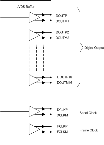
A graphical representation of the 18 LVDS output buffers is shown in Figure 70.
 Figure 70. LVDS Output
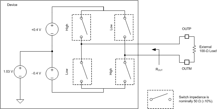
The equivalent circuit of each LVDS output buffer is shown in Figure 71. The buffer is designed for a differential output impedance of 100 Ω (ROUT). The differential outputs can be terminated at the receiver end by a 100-Ω termination. The buffer output impedance functions like a source-side series termination. By absorbing reflections from the receiver end, the buffer output impedance helps improve signal integrity.

NOTE: When either the high or low switches are closed, differential ROUT = 100 Ω.
Figure 71. LVDS Output Circuit