JAJSFC6C May 2015 – April 2018 ADS52J90
PRODUCTION DATA.
- 1 特長
- 2 アプリケーション
- 3 概要
- 4 改訂履歴
- 5 概要(続き)
- 6 Pin Configuration and Functions
-
7 Specifications
- 7.1 Absolute Maximum Ratings
- 7.2 ESD Ratings
- 7.3 Recommended Operating Conditions
- 7.4 Thermal Information
- 7.5 Electrical Characteristics
- 7.6 Digital Characteristics
- 7.7 Timing Requirements: Signal Chain
- 7.8 Timing Requirements: JESD Interface
- 7.9 Timing Requirements: Serial Interface
- 7.10 Typical Characteristics
- 7.11 Typical Characteristics: JESD Interface
- 7.12 Typical Characteristics: Contour Plots
-
8 Detailed Description
- 8.1 Overview
- 8.2 Functional Block Diagrams
- 8.3
Feature Description
- 8.3.1 Connection of the External Inputs to the Input Pins
- 8.3.2 Input Multiplexer and Sampler
- 8.3.3 Analog-to-Digital Converter (ADC)
- 8.3.4 Device Synchronization Using TX_TRIG
- 8.3.5 Digital Processing
- 8.3.6 Data Formatting
- 8.3.7 Serializer and LVDS Interface
- 8.3.8 LVDS Buffers
- 8.3.9 JESD204B Interface
- 8.3.10 Interfacing SYNC~ and SYSREF Between the FPGA and ADCs
- 8.3.11 Clock Input
- 8.3.12 Analog Input and Driving Circuit
- 8.4 Device Functional Modes
- 8.5 Programming
- 9 Application and Implementation
- 10Power Supply Recommendations
- 11Layout
-
12Register Map
- 12.1
ADC Registers
- 12.1.1
Description of Registers
- 12.1.1.1 Register 0h (address = 0h)
- 12.1.1.2 Register 1h (address = 1h)
- 12.1.1.3 Register 2h (address = 2h)
- 12.1.1.4 Register 3h (address = 3h)
- 12.1.1.5 Register 4h (address = 4h)
- 12.1.1.6 Register 5h (address = 5h)
- 12.1.1.7 Register 7h (address = 7h)
- 12.1.1.8 Register 8h (address = 8h)
- 12.1.1.9 Register Ah (address = Ah)
- 12.1.1.10 Register Bh (address = Bh)
- 12.1.1.11 Register Dh (address = Dh)
- 12.1.1.12 Register Eh (address = Eh)
- 12.1.1.13 Register Fh (address = Fh)
- 12.1.1.14 Register 10h (address = 10h)
- 12.1.1.15 Register 11h (address = 11h)
- 12.1.1.16 Register 12h (address = 12h)
- 12.1.1.17 Register 13h (address = 13h)
- 12.1.1.18 Register 14h (address = 14h)
- 12.1.1.19 Register 15h (address = 15h)
- 12.1.1.20 Register 17h (address = 17h)
- 12.1.1.21 Register 18h (address = 18h)
- 12.1.1.22 Register 19h (address = 19h)
- 12.1.1.23 Register 1Ah (address = 1Ah)
- 12.1.1.24 Register 1Bh (address = 1Bh)
- 12.1.1.25 Register 1Ch (address = 1Ch)
- 12.1.1.26 Register 1Dh (address = 1Dh)
- 12.1.1.27 Register 1Eh (address = 1Eh)
- 12.1.1.28 Register 1Fh (address = 1Fh)
- 12.1.1.29 Register 20h (address = 20h)
- 12.1.1.30 Register 21h (offset = 21h)
- 12.1.1.31 Register 23h (register = 23h)
- 12.1.1.32 Register 24h (address = 24h)
- 12.1.1.33 Register 25h (address = 25h)
- 12.1.1.34 Register 26h (address = 26h)
- 12.1.1.35 Register 27h (address = 27h)
- 12.1.1.36 Register 28h (address = 28h)
- 12.1.1.37 Register 29h (address = 29h)
- 12.1.1.38 Register 2Ah (address = 2Ah)
- 12.1.1.39 Register 2Bh (address = 2Bh)
- 12.1.1.40 Register 2Ch (address = 2Ch)
- 12.1.1.41 Register 2Dh (address = 2Dh)
- 12.1.1.42 Register 2Fh (address = 2Fh)
- 12.1.1.43 Register 30h (address = 30h)
- 12.1.1.44 Register 31h (address = 31h)
- 12.1.1.45 Register 32h (address = 32h)
- 12.1.1.46 Register 33h (address = 33h)
- 12.1.1.47 Register 34h (address = 34h)
- 12.1.1.48 Register 35h (address = 35h)
- 12.1.1.49 Register 36h (address = 36h)
- 12.1.1.50 Register 37h (address = 37h)
- 12.1.1.51 Register 38h (address = 38h)
- 12.1.1.52 Register 39h (address = 39h)
- 12.1.1.53 Register 3Bh (address = 3Bh)
- 12.1.1.54 Register 3Ch (address = 3Ch)
- 12.1.1.55 Register 43h (address = 43h)
- 12.1.1
Description of Registers
- 12.2
JESD Serial Interface Registers
- 12.2.1
Description of JESD Serial Interface Registers
- 12.2.1.1 Register 70 (address = 46h)
- 12.2.1.2 Register 73 (address = 49h)
- 12.2.1.3 Register 74 (address = 4Ah)
- 12.2.1.4 Register 75 (address = 4Bh)
- 12.2.1.5 Register 77 (address = 4Dh)
- 12.2.1.6 Register 80 (address = 50h)
- 12.2.1.7 Register 81 (address = 51h)
- 12.2.1.8 Register 82 (address = 52h)
- 12.2.1.9 Register 83 (address = 53h)
- 12.2.1.10 Register 85 (address = 55h)
- 12.2.1.11 Register 115 (address = 73h)
- 12.2.1.12 Register 116 (address = 74h)
- 12.2.1.13 Register 117 (address = 75h)
- 12.2.1.14 Register 118 (address = 76h)
- 12.2.1.15 Register 119 (address = 77h)
- 12.2.1.16 Register 120 (address = 78h)
- 12.2.1.17 Register 134 (address = 86h)
- 12.2.1.18 Register 135 (address = 87h)
- 12.2.1.19 Register 136 (address = 88h)
- 12.2.1.20 Register 137 (address = 89h)
- 12.2.1.21 Register 138 (address = 8Ah)
- 12.2.1
Description of JESD Serial Interface Registers
- 12.1
ADC Registers
- 13デバイスおよびドキュメントのサポート
- 14メカニカル、パッケージ、および注文情報
8.3.10 Interfacing SYNC~ and SYSREF Between the FPGA and ADCs
The SYNC~ and SYSREF signals must be connected to the FPGA and the multiple ADCs in the system. When driving SYNC~ and SYSREF using differential signals, additional interface circuits may be required to decouple the common-mode levels between the FPGA and the ADC. Figure 80 shows an overview of such a scheme for driving the SYNC~ signal from the FPGA to multiple ADCs.
 Figure 80. Connection of SYNC~ From the FPGA to the ADCs
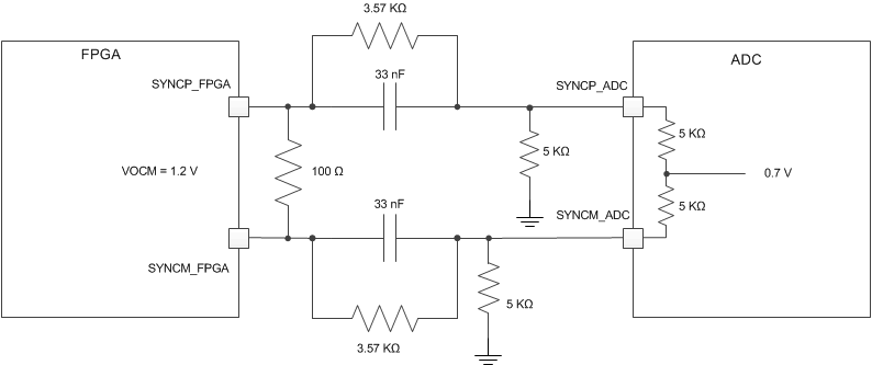
The ADC has internal 5-kΩ resistors from the SYNCP and SYNCM pins to an internal reference voltage of 0.7 V. When driven by a differential driver, an interface circuit may be required to match the common-mode voltages between the driver and the ADC. An example circuit is shown in Figure 81 to level-shift from a 1.2-V common-mode voltage at the driver output to the 0.7 V at the ADC input. The 100 Ω at the driver output depicts the differential termination and could be realized inside the FPGA.
 Figure 81. Circuit to Level-Shift the Common-Mode Voltage From 1.2 V at the Driver Output to 0.7 V at the ADC Input
For a different driver output common-mode than the one shown in Figure 81, the interface circuit must be modified.
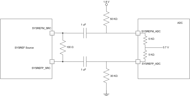
A similar circuit as shown in Figure 81 can also be used to interface the SYSREF signals to the ADC. As shown in Figure 82, the SYSREF signal can also be driven using an ac-coupling scheme. The external components are chosen for a case where the SYSREF source drives only one ADC. The values of these components must be changed if the signal is interfaced to multiple ADCs (contact the factory for details).
 Figure 82. AC-Coupling Scheme for SYSREF (do not use for SYNC~)
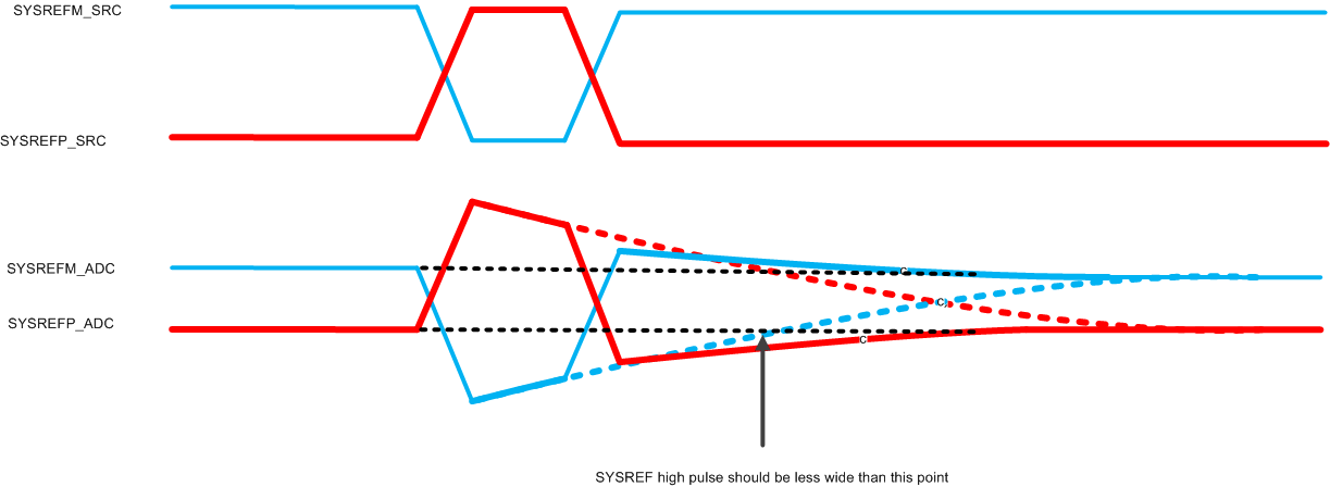
 Figure 83. Transient of SYSREF With AC-Coupling
The 50-kΩ and 30-kΩ external resistors along with the two 5-kΩ resistors internal to the ADC form a voltage divider circuit to generate a negative differential offset at the ADC SYSREF input when SYSREF is low. A high-going pulse on the SYSREF_SRC signal passes through the ac-coupling capacitor. The ac-coupling capacitor and the resistors form a high-pass filter and cause the SYSREF_ADC signal to droop towards their quiescent values over time (denoted by the dotted lines in Figure 83). However, if the high width of SYSREF is much lower than the time constant of the filter, the circuit is able to pass the pulse properly.
The SYNC~ and SYSREF signals also can be driven using single-ended LVCMOS levels, which can be done by driving the P side with the LVCMOS level and connecting the M side to ground as shown in Figure 84. When driven in this manner, the internal 5-kΩ resistor (connecting the P and M pins to the 0.7-V node) is disconnected from the pins.
 Figure 84. Single-Ended Driving Circuit for SYNC~ and SYSREF