SLAS669E September 2010 – may 2020 ADS5400-SP
PRODUCTION DATA.
- 1 Features
- 2 Applications
- 3 Description
- 4 Revision History
- 5 Pin Configuration and Functions
- 6 Specifications
-
7 Detailed Description
- 7.1 Overview
- 7.2 Functional Block Diagram
- 7.3 Feature Description
- 7.4 Device Functional Modes
- 7.5 Programming
- 7.6 Serial Register Map
- 8 Application and Implementation
- 9 Power Supply Recommendations
- 10Layout
- 11Device and Documentation Support
- 12Mechanical, Packaging, and Orderable Information
7.3.1 Input Configuration
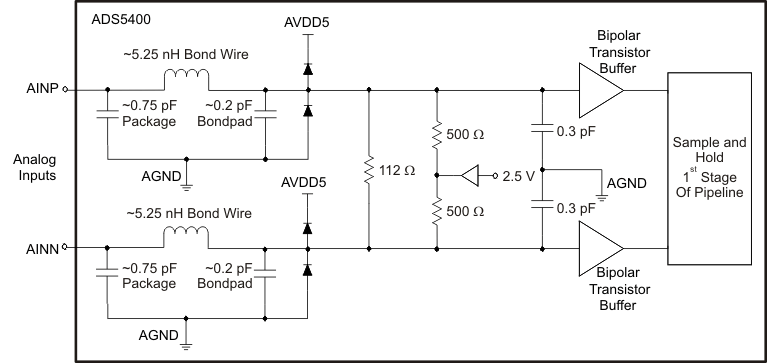
The analog input for the ADS5400-SP consists of an analog pseudo-differential buffer followed by a bipolar transistor track-and-hold (see Figure 25). The integrated analog buffer isolates the source driving the input of the ADC from sampling glitches on the T&H and allows for the integration of a 100-Ω differential input resistor. The input common mode is set internally through a 500-Ω resistor connected from half of the AVDD5 supply voltage to each of the inputs. The parasitic package capacitance shown is with the package unsoldered. Once soldered, depending on the board characteristics, one can expect another ~1pF at the analog input pins, which is board dependent.
 Figure 25. Analog Input Equivalent Circuit
 For a full-scale differential input, each of the differential lines of the input signal swing symmetrically between 2.5 V + 0.5 V and 2.5 V – 0.5 V. This means that each input has a maximum signal swing of 1 VPP for a total differential input signal swing of 2 VPP. The maximum fullscale range can be programmed from 1.5-2Vpp using the SPI. The maximum swing is determined by the internal reference voltage generator and the fullscale range set using the SPI, eliminating the need for any external circuitry for this purpose. The analog gain adjustment has a resolution of 12-bits across the 1.5-2VPP range, providing for fine calibration of analog gain mismatches across multiple ADS5400-SP signal chains, primarily for interleaving.
The ADS5400-SP obtains optimum performance when the analog inputs are driven differentially. The circuit in Figure 26 shows one possible configuration using an RF transformer. Datasheet performance, especially at >1GHz input frequency, can only be obtained with a carefully designed differential drive path to the ADC.
 Figure 26. Converting a Single-Ended Input to a Differential Signal Using an RF Transformer