SBAS713C May 2015 – January 2017 ADS54J69
PRODUCTION DATA.
- 1 Features
- 2 Applications
- 3 Description
- 4 Revision History
- 5 Device Comparison Table
- 6 Pin Configuration and Functions
- 7 Specifications
-
8 Detailed Description
- 8.1 Overview
- 8.2 Functional Block Diagram
- 8.3 Feature Description
- 8.4 Device Functional Modes
- 8.5
Register Maps
- 8.5.1 Detailed Register Info
- 8.5.2 Example Register Writes
- 8.5.3
Register Descriptions
- 8.5.3.1 General Registers
- 8.5.3.2
Master Page (080h) Registers
- 8.5.3.2.1 Register 20h (address = 20h), Master Page (080h)
- 8.5.3.2.2 Register 21h (address = 21h), Master Page (080h)
- 8.5.3.2.3 Register 23h (address = 23h), Master Page (080h)
- 8.5.3.2.4 Register 24h (address = 24h), Master Page (080h)
- 8.5.3.2.5 Register 26h (address = 26h), Master Page (080h)
- 8.5.3.2.6 Register 39h (address = 39h), Master Page (080h)
- 8.5.3.2.7 Register 3Ah (address = 3Ah), Master Page (080h)
- 8.5.3.2.8 Register 4Fh (address = 4Fh), Master Page (080h)
- 8.5.3.2.9 Register 53h (address = 53h), Master Page (080h)
- 8.5.3.2.10 Register 54h (address = 54h), Master Page (080h)
- 8.5.3.2.11 Register 55h (address = 55h), Master Page (080h)
- 8.5.3.2.12 Register 56h (address = 56h), Master Page (080h)
- 8.5.3.2.13 Register 59h (address = 59h), Master Page (080h)
- 8.5.3.3 ADC Page (0Fh) Registers
- 8.5.3.4
Main Digital Page (6800h) Registers
- 8.5.3.4.1 Register 0h (address = 0h), Main Digital Page (6800h)
- 8.5.3.4.2 Register 41h (address = 41h), Main Digital Page (6800h)
- 8.5.3.4.3 Register 42h (address = 42h), Main Digital Page (6800h)
- 8.5.3.4.4 Register 43h (address = 43h), Main Digital Page (6800h)
- 8.5.3.4.5 Register 44h (address = 44h), Main Digital Page (6800h)
- 8.5.3.4.6 Register 4Bh (address = 4Bh), Main Digital Page (6800h)
- 8.5.3.4.7 Register 4Dh (address = 4Dh), Main Digital Page (6800h)
- 8.5.3.4.8 Register 4Eh (address = 4Eh), Main Digital Page (6800h)
- 8.5.3.4.9 Register 52h (address = 52h), Main Digital Page (6800h)
- 8.5.3.4.10 Register 72h (address = 72h), Main Digital Page (6800h)
- 8.5.3.4.11 Register ABh (address = ABh), Main Digital Page (6800h)
- 8.5.3.4.12 Register ADh (address = ADh), Main Digital Page (6800h)
- 8.5.3.4.13 Register F7h (address = F7h), Main Digital Page (6800h)
- 8.5.3.5
JESD Digital Page (6900h) Registers
- 8.5.3.5.1 Register 0h (address = 0h), JESD Digital Page (6900h)
- 8.5.3.5.2 Register 1h (address = 1h), JESD Digital Page (6900h)
- 8.5.3.5.3 Register 2h (address = 2h), JESD Digital Page (6900h)
- 8.5.3.5.4 Register 3h (address = 3h), JESD Digital Page (6900h)
- 8.5.3.5.5 Register 5h (address = 5h), JESD Digital Page (6900h)
- 8.5.3.5.6 Register 6h (address = 6h), JESD Digital Page (6900h)
- 8.5.3.5.7 Register 7h (address = 7h), JESD Digital Page (6900h)
- 8.5.3.5.8 Register 31h (address = 31h), JESD Digital Page (6900h)
- 8.5.3.5.9 Register 32h (address = 32h), JESD Digital Page (6900h)
- 8.5.3.6 JESD Analog Page (6A00h) Register
- 9 Application and Implementation
- 10Power Supply Recommendations
- 11Layout
- 12Device and Documentation Support
- 13Mechanical, Packaging, and Orderable Information
8 Detailed Description
8.1 Overview
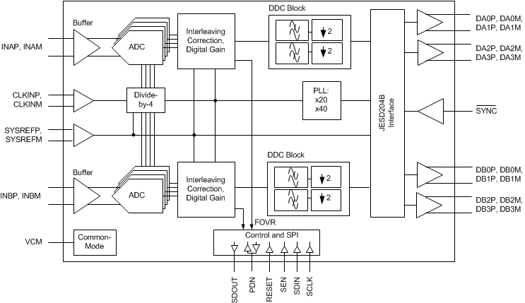
The ADS54J69 is a low-power, wide-bandwidth, 16-bit, 500-MSPS, dual-channel, analog-to-digital converter (ADC). The ADS54J69 employs four interleaving ADCs for each channel to achieve a noise floor of –159 dBFS/Hz.
The ADS54J69 uses TI's proprietary interleaving and dither algorithms to achieve a clean spectrum with high spurious-free dynamic range (SFDR). Built-in, half-band, decimate-by-2 filters further enhance the capability of the ADS54J69 to deliver excellent signal-to-noise ratio (SNR) and SFDR over a wide range of frequencies. Analog input buffers isolate the ADC driver from glitch energy generated from sampling process, thereby simplify the driving network on-board.
The JESD204B interface reduces the number of interface lines with two-lane and four-lane options, allowing a high system integration density. The JESD204B interface operates in subclass-1, enabling multi-chip synchronization with the SYSREF input.
8.2 Functional Block Diagram
8.3 Feature Description
8.3.1 Analog Inputs
The ADS54J69 analog signal inputs are designed to be driven differentially. The analog input pins have internal analog buffers that drive the sampling circuit. As a result of the analog buffer, the input pins present a high impedance input across a very wide frequency range to the external driving source that enables great flexibility in the external analog filter design as well as excellent 50-Ω matching for RF applications. The buffer also helps isolate the external driving circuit from the internal switching currents of the sampling circuit, resulting in a more constant SFDR performance across input frequencies.
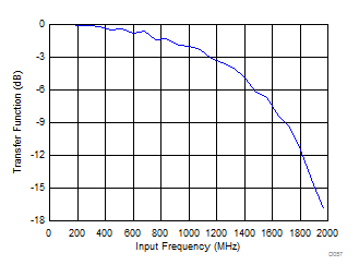
The common-mode voltage of the signal inputs is internally biased to VCM using 600-Ω resistors, allowing for ac-coupling of the input drive network. Each input pin (INP, INM) must swing symmetrically between (VCM + 0.475 V) and (VCM – 0.475 V), resulting in a 1.9-VPP (default) differential input swing. The input sampling circuit has a 3-dB bandwidth that extends up to 1.2 GHz. An equivalent analog input network diagram is shown in Figure 59.
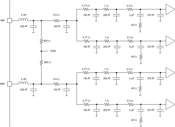 Figure 59. Analog Input Network
The input bandwidth shown in Figure 60 is measured with respect to a 50-Ω differential input termination at the ADC input pins.
8.3.2 DDC Block
The ADS54J69 has an optional DDC block that can be enabled via an SPI register write. Each ADC channel is followed by a DDC block consisting of a decimate-by-2, half-band, finite impulse response (FIR) filter with low-pass and high-pass options programmable via the SPI interface.
8.3.2.1 Decimate-by-2 Filter
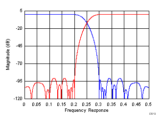
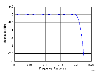
This decimation filter has 41 taps. The stop-band attenuation is approximately 90 dB and the pass-band flatness is ±0.05 dB. Table 1 shows corner frequencies for the low-pass and high-pass filter options.
Table 1. Corner Frequencies for the Decimate-by-2 Filter
| CORNERS (dB) | LOW PASS | HIGH PASS |
|---|---|---|
| –0.1 | 0.202 × fS | 0.298 × fS |
| –0.5 | 0.210 × fS | 0.290 × fS |
| –1 | 0.215 × fS | 0.285 × fS |
| –3 | 0.227 × fS | 0.273 × fS |
Figure 61 and Figure 62 show the frequency response of the decimate-by-2 filter from dc to fS / 2.
8.3.3 SYSREF Signal
The SYSREF signal is a periodic signal that is sampled by the ADS54J69 device clock and used to align the boundary of the local multi-frame clock inside the data converter. SYSREF is required to be a sub-harmonic of the local multi-frame clock (LMFC) internal timing. To meet this requirement, the timing of SYSREF is dependent on the device clock frequency and the LMFC frequency, as determined by the selected DDC decimation and frames per multi-frame settings. The SYSREF signal is recommended be a low-frequency signal in the range of 1 MHz to 5 MHz in order to reduce coupling to the signal path both on the printed circuit board (PCB) as well as internal in the device.
The external SYSREF signal must be a sub-harmonic of the internal LMFC clock, as shown in Equation 1 and Table 2.
where
- N = 0, 1, 2, and so forth
Table 2. LMFC Clock Frequency
| LMFS CONFIGURATION | DECIMATION | LMFC CLOCK(1)(2) |
|---|---|---|
| 4222 | 2X | (fS / 4) / k |
| 2242 | 2X | (fS / 4) / k |
8.3.3.1 SYSREF Not Present (Subclass 0, 2)
A SYSREF pulse is required by the ADS54J69 to reset internal counters. If SYSREF is not present, as can be the case in subclass 0 or 2, this pulse can be done by doing the following register writes shown in Table 3.
Table 3. Internally Pulsing SYSREF Twice Using Register Writes
| ADDRESS (Hex) | DATA (Hex) | COMMENT |
|---|---|---|
| 0-011h | 80h | Set the master page |
| 0-054h | 80h | Enable manual SYSREF |
| 0-053h | 01h | Set SYSREF high |
| 0-053h | 00h | Set SYSREF low |
| 0-053h | 01h | Set SYSREF high |
| 0-053h | 00h | Set SYSREF low |
8.3.4 Overrange Indication
The ADS54J69 provides a fast overrange indication that can be presented in the digital output data stream via an SPI configuration. Alternatively, if not used, the SDOUT (pin 11) and PDN (pin 50) pins can be configured via the SPI to output the fast overrange (FOVR) indicator.
When the FOVR indication is embedded in the output data stream, the FOVR replaces the LSB of the 16-bit data stream going to the 8b/10b encoder, as shown in Figure 63.
 Figure 63. Overrange Indication in a Data Stream
8.3.4.1 Fast OVR
The fast OVR is triggered if the input voltage exceeds the programmable overrange threshold and is presented after only 18 clock cycles + tPD (tPD of the gates and buffers is approximately 4 ns), thus enabling a quicker reaction to an overrange event.
The input voltage level at which the overload is detected is referred to as the threshold. The threshold is programmable using the FOVR THRESHOLD bits, as shown in Figure 64. The FOVR is triggered 18 clock cycles + tPD (tPD of the gates and buffers is approximately 4 ns) after the overload condition occurs.
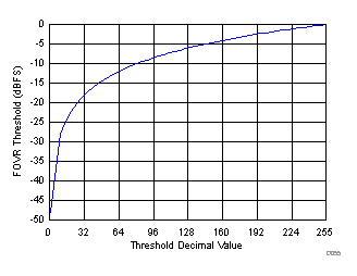
The input voltage level at which the fast OVR is triggered is defined by Equation 2:
The default threshold is E3h (227d), corresponding to a threshold of –1 dBFS.
In terms of full-scale input, the fast OVR threshold can be calculated as Equation 3:
8.3.5 Power-Down Mode
The ADS54J69 provides a highly-configurable power-down mode. Power-down can be enabled by using the PDN pin or via SPI register writes.
A power-down mask can be configured that allows a trade-off between wake-up time and power consumption in power-down mode. Two independent power-down masks can be configured: MASK 1 and MASK 2, as shown in Table 4. See the master page registers in Table 10 for further details.
Table 4. Register Address for Power-Down Modes
| REGISTER ADDRESS | COMMENT | REGISTER DATA | |||||||
|---|---|---|---|---|---|---|---|---|---|
| A[7:0] (Hex) | 7 | 6 | 5 | 4 | 3 | 2 | 1 | 0 | |
| MASTER PAGE (80h) | |||||||||
| 20 | MASK 1 | PDN ADC CHA | PDN ADC CHB | ||||||
| 21 | PDN BUFFER CHB | PDN BUFFER CHA | 0 | 0 | 0 | 0 | |||
| 23 | MASK 2 | PDN ADC CHA | PDN ADC CHB | ||||||
| 24 | PDN BUFFER CHB | PDN BUFFER CHA | 0 | 0 | 0 | 0 | |||
| 26 | CONFIG | GLOBAL PDN | OVERRIDE PDN PIN | PDN MASK SEL | 0 | 0 | 0 | 0 | 0 |
| 53 | 0 | MASK SYSREF | 0 | 0 | 0 | 0 | 0 | 0 | |
| 55 | 0 | 0 | 0 | PDN MASK | 0 | 0 | 0 | 0 | |
To save power, the device can be put in complete power-down by using the GLOBAL PDN register bit. However, when the JESD link is required to be active during power-down, the ADC and analog buffer can be selectively powered down by using the PDN ADC CHx and PDN BUFFER CHx register bits after enabling the PDN MASK register bit. The PDN MASK SEL register bit can be used to select between MASK 1 or MASK 2. Table 5 shows power consumption for different combinations of the GLOBAL PDN, PDN ADC CHx, and PDN BUFF CHx register bits.
Table 5. Power Consumption in Different Power-Down Settings
| REGISTER BIT | COMMENT | IAVDD3V (mA) | IAVDD (mA) | IDVDD (mA) | IIOVDD (mA) | TOTAL POWER (W) |
|---|---|---|---|---|---|---|
| Default | After reset, with a full-scale input signal to both channels | 346 | 354 | 188 | 512 | 2.66 |
| GBL PDN = 1 | The device is in a complete power-down state | 3 | 6 | 21 | 127 | 0.2 |
| GBL PDN = 0, PDN ADC CHx = 1 (x = A or B) |
The ADC of one channel is powered down | 284 | 221 | 130 | 461 | 2.05 |
| GBL PDN = 0, PDN BUFF CHx = 1 (x = A or B) |
The input buffer of one channel is powered down | 270 | 352 | 188 | 516 | 2.43 |
| GBL PDN = 0, PDN ADC CHx = 1, PDN BUFF CHx = 1 (x = A or B) |
The ADC and input buffer of one channel are powered down | 206 | 220 | 129 | 465 | 1.82 |
| GBL PDN = 0, PDN ADC CHx = 1, PDN BUFF CHx = 1 (x = A and B) |
The ADC and input buffer of both channels are powered down | 64 | 84 | 67 | 389 | 0.93 |
8.4 Device Functional Modes
8.4.1 Device Configuration
The ADS54J69 can be configured by using a serial programming interface, as described in the Serial Interface section. In addition, the device has one dedicated parallel pin (PDN) for controlling the power-down mode.
The ADS54J69 supports a 24-bit (16-bit address, 8-bit data) SPI operation and uses paging (see the Register Maps section) to access all register bits.
8.4.1.1 Serial Interface
The ADC has a set of internal registers that can be accessed by the serial interface formed by the SEN (serial interface enable), SCLK (serial interface clock), and SDIN (serial interface data) pins, as shown in Figure 65. Legends used in Figure 65 are explained in Table 6. Serially shifting bits into the device is enabled when SEN is low. Serial data on SDIN are latched at every SCLK rising edge when SEN is active (low). The interface can function with SCLK frequencies from 2 MHz down to very low speeds (of a few Hertz) and also with a non-50% SCLK duty cycle.
 Figure 65. SPI Timing Diagram
Table 6. SPI Timing Diagram Legend
| SPI BITS | DESCRIPTION | BIT SETTINGS |
|---|---|---|
| R/W | Read/write bit | 0 = SPI write 1 = SPI read back |
| M | SPI bank access | 0 = Analog SPI bank (master and ADC pages) 1 = JESD SPI bank (main digital, analog JESD, and digital JESD pages) |
| P | JESD page selection bit | 0 = Page access 1 = Register access |
| CH | SPI access for a specific channel of the JESD SPI bank | 0 = Channel A 1 = Channel B By default, both channels are being addressed. |
| A[11:0] | SPI address bits | — |
| D[7:0] | SPI data bits | — |
Table 7 shows the timing requirements for the serial interface signals in Figure 65.
Table 7. SPI Timing Requirements
| MIN | TYP | MAX | UNIT | ||
|---|---|---|---|---|---|
| fSCLK | SCLK frequency (equal to 1 / tSCLK) | > dc | 2 | MHz | |
| tSLOADS | SEN to SCLK setup time | 100 | ns | ||
| tSLOADH | SCLK to SEN hold time | 100 | ns | ||
| tDSU | SDIN setup time | 100 | ns | ||
| tDH | SDIN hold time | 100 | ns | ||
8.4.1.2 Serial Register Write: Analog Bank
The analog SPI bank contains two pages (the master and ADC page). The internal register of the ADS54J69 analog SPI bank can be programmed by:
- Driving the SEN pin low.
- Initiating a serial interface cycle specifying the page address of the register whose content must be written.
- Master page: write address 0011h with 80h.
- ADC page: write address 0011h with 0Fh.
- Writing the register content, as shown in Figure 66. When a page is selected, multiple writes into the same page can be done.
 Figure 66. Serial Register Write Timing Diagram
8.4.1.3 Serial Register Readout: Analog Bank
The content from one of the two analog banks can be read out by:
- Driving the SEN pin low.
- Selecting the page address of the register whose content must be read.
- Master page: write address 0011h with 80h.
- ADC page: write address 0011h with 0Fh.
- Setting the R/W bit to 1 and writing the address to be read back.
- Reading back the register content on the SDOUT pin, as shown in Figure 67. When a page is selected, multiple read backs from the same page can be done.
 Figure 67. Serial Register Read Timing Diagram
8.4.1.4 JESD Bank SPI Page Selection
The JESD SPI bank contains four pages (main digital, digital, and analog JESD pages). The individual pages can be selected by:
- Driving the SEN pin low.
- Setting the M bit to 1 and specifying the page with two register writes. Note that the P bit must be set to 0, as shown in Figure 68.
- Write address 4003h with 00h (LSB byte of page address).
- Write address 4004h with the MSB byte of the page address.
- For the main digital page: write address 4004h with 68h.
- For the digital JESD page: write address 4004h with 69h.
- For the analog JESD page: write address 4004h with 6Ah.
 Figure 68. SPI Page Selection
8.4.1.5 Serial Register Write: JESD Bank
The ADS54J69 is a dual-channel device and the JESD204B portion is configured individually for each channel by using the CH bit. Note that the P bit must be set to 1 for register writes.
- Drive the SEN pin low.
- Select the JESD bank page. Note that the M bit = 1 and the P bit = 0.
- Write address 4003h with 00h.
- If separate control for both channels is desired, write address 4005h with 01h.
- For the main digital page: write address 4004h with 68h.
- For the digital JESD page: write address 4004h with 69h.
- For the analog JESD page: write address 4004h with 6Ah.
- Set the M and P bits to 1, select channel A (CH = 0) or channel B (CH = 1), and write the register content as shown in Figure 69. When a page is selected, multiple writes into the same page can be done.
 Figure 69. JESD Serial Register Write Timing Diagram
8.4.1.5.1 Individual Channel Programming
By default, register writes are applied to both channels. To enable individual channel writes, write address 4005h with 01h (default is 00h).
8.4.1.6 Serial Register Readout: JESD Bank
The content from one of the pages of the JESD bank can be read out by:
- Driving the SEN pin low.
- Select the JESD bank page. Note that the M bit = 1 and the P bit = 0.
- Write address 4003h with 00h.
- If separate control for both channels is desired, write address 4005h with 01h.
- For the main digital page: write address 4004h with 68h.
- For the digital JESD page: write address 4004h with 69h.
- For the analog JESD page: write address 4004h with 6Ah.
- Setting the R/W, M, and P bits to 1, selecting channel A or channel B, and writing the address to be read back.
- Reading back the register content on the SDOUT pin; see Figure 70. When a page is selected, multiple read backs from the same page can be done.
 Figure 70. JESD Serial Register Read Timing Diagram
8.4.2 JESD204B Interface
The ADS54J69 supports device subclass 1 with a maximum output data rate of 10.0 Gbps for each serial transmitter.
An external SYSREF signal is used to align all internal clock phases and the local multi-frame clock to a specific sampling clock edge, allowing synchronization of multiple devices in a system and minimizing timing and alignment uncertainty. The SYNC input is used to control the JESD204B SERDES blocks.
Depending on the ADC output data rate, the JESD204B output interface can be operated with either two or four active lanes (out of total 8 lanes), as shown in Figure 71. The JESD204B setup and configuration of the frame assembly parameters is controlled via the SPI interface.
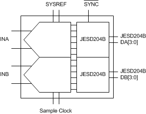 Figure 71. ADS54J69 Block Diagram
The JESD204B transmitter block shown in Figure 72 consists of the transport layer, the data scrambler, and the link layer. The transport layer maps the ADC output data into the selected JESD204B frame data format. The link layer performs the 8b/10b data encoding as well as the synchronization and initial lane alignment using the SYNC input signal. Optionally, data from the transport layer can be scrambled.
 Figure 72. JESD204B Transmitter Block
8.4.2.1 JESD204B Initial Lane Alignment (ILA)
The initial lane alignment process is started when the receiving device de-asserts the SYNC signal, as shown in Figure 73. When a logic low is detected on the SYNC input pin, the ADS54J69 starts transmitting comma (K28.5) characters to establish a code group synchronization.
When synchronization is complete, the receiving device asserts the SYNC signal and the ADS54J69 starts the initial lane alignment sequence with the next local multi-frame clock boundary. The ADS54J69 transmits four multi-frames, each containing K frames (K is SPI programmable). Each of the multi-frames contains the frame start and end symbols and the second multi-frame also contains the JESD204 link configuration data.
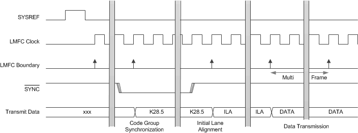 Figure 73. Lane Alignment Sequence
8.4.2.2 JESD204B Test Patterns
There are three different test patterns available in the transport layer of the JESD204B interface. The ADS54J69 supports a clock output, encoded, and a PRBS (215 – 1) pattern. These test patterns can be enabled via an SPI register write and are located in the JESD digital page of the JESD bank.
8.4.2.3 JESD204B Frame
The JESD204B standard defines the following parameters:
- L is the number of lanes per link
- M is the number of converters per device
- F is the number of octets per frame clock period, per lane
- S is the number of samples per frame per converter
8.4.2.4 JESD204B Frame Assembly with Decimation
Table 8 lists the available JESD204B formats and interface rate at maximum sampling frequency. At lower sampling frequencies, interface rates scale down proportionally.
Figure 74 shows the detailed frame assembly for the decimated output.
Table 8. Interface Rates with Decimation Filter
| L | M | F | S | JESD MODE REGISTER BIT | JESD PLL MODE SETTING | DECIMATION | MAX ADC OUTPUT RATE (MSPS) | MAX fSERDES (Gbps) |
|---|---|---|---|---|---|---|---|---|
| 4 | 2 | 2 | 2 | 001 | 20x | 2X | 500 | 5.0 |
| 2 | 2 | 4 | 2 | 010 | 40x | 2X | 500 | 10.0 |
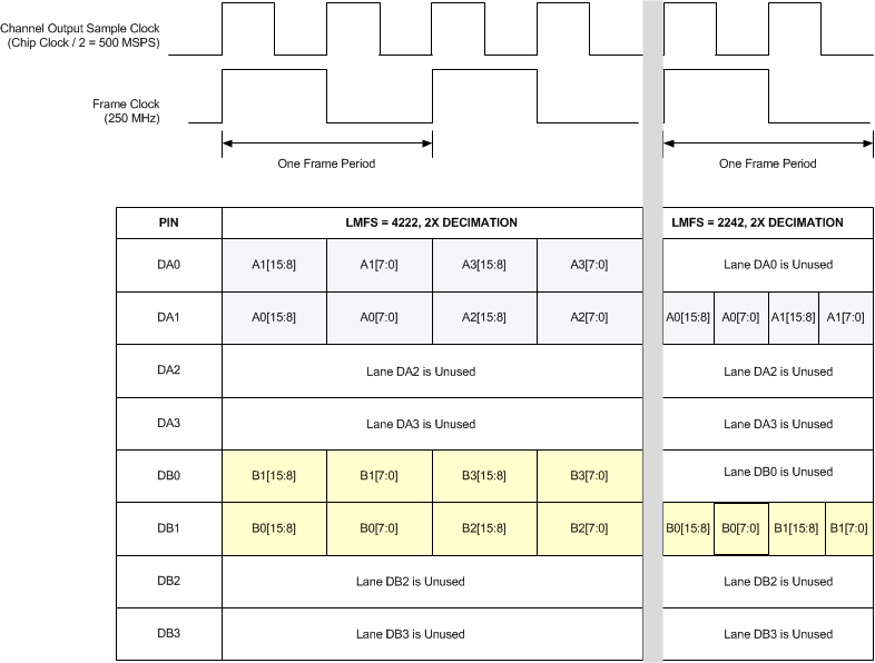 Figure 74. Frame Assembly with Decimation Filter
Note that after power-up, the JESD output bus must be reordered to obtain correct link parameters in the ILA sequence. Table 9 shows the required register writes to reorder the JESD output bus.
Table 9. Configuring LMFS for the JESD Link
| L | M | F | S | DECIMATION | JESD PLL MODE (In JESD Analog Page) |
JESD MODE REGISTER BIT (In JESD Digital Page) |
DA_BUS_REORDER REGISTER BIT (In JESD Digital Page) |
DB_BUS_REORDER REGISTER BIT (In JESD Digital Page) |
REGISTER 52 (In Main Digital Page) |
REGISTER 72 (In Main Digital Page) |
|---|---|---|---|---|---|---|---|---|---|---|
| 4 | 2 | 2 | 2 | 2X | 00h | 01h | 0Ah | 0Ah | 80h | 08h |
| 2 | 2 | 4 | 2 | 2X | 10h | 02h | 0Ah | 0Ah | 80h | 08h |
8.4.2.4.1 JESD Transmitter Interface
Each of the 10.0-Gbps SERDES JESD transmitter outputs requires ac-coupling between the transmitter and receiver. The differential pair must be terminated with 100-Ω resistors as close to the receiving device as possible to avoid unwanted reflections and signal degradation, as shown in Figure 75.
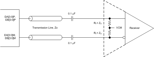 Figure 75. Output Connection to Receiver
8.4.2.4.2 Eye Diagrams
Figure 76 to Figure 79 show the serial output eye diagrams of the ADS54J69 at 5.0 Gbps and 10 Gbps with default and increased output voltage swing against the JESD204B mask.
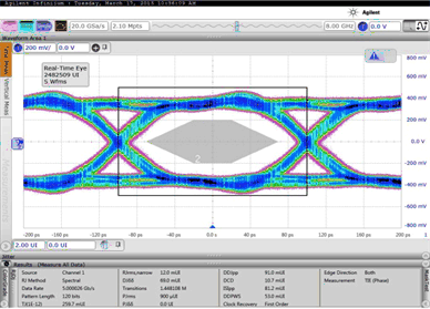 Figure 76. Eye Diagram at 5-Gbps Bit Rate with
 Default Output Swing
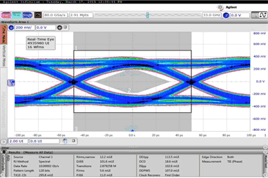 Figure 78. Eye Diagram at 10-Gbps Bit Rate with
 Default Output Swing
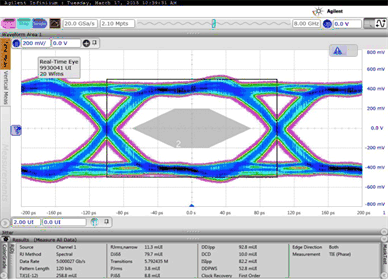 Figure 77. Eye Diagram at 5-Gbps Bit Rate with
 Increased Output Swing
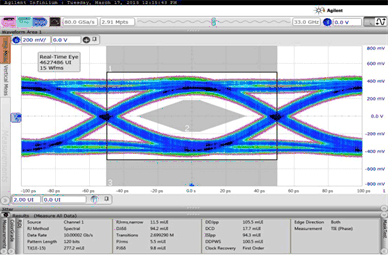 Figure 79. Eye Diagram at 10-Gbps Bit Rate with
 Increased Output Swing
8.5 Register Maps
Figure 80 shows a conceptual diagram of the serial registers.
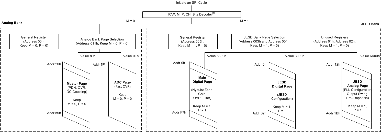 Figure 80. Serial Interface Registers
8.5.1 Detailed Register Info
The ADS54J69 contains two main SPI banks: the analog SPI bank and the digital SPI bank. The analog SPI bank gives access to the ADC analog blocks and the JESD SPI bank controls the digital features and anything related to the JESD204B serial interface. The analog SPI bank is divided into two pages (master and ADC) and the JESD SPI bank is divided into three pages (main digital, JESD digital, and JESD analog). Table 10 lists a register map for the ADS54J69.
Table 10. Register Map
| REGISTER ADDRESS | REGISTER DATA | |||||||
|---|---|---|---|---|---|---|---|---|
| A[11:0] (Hex) | 7 | 6 | 5 | 4 | 3 | 2 | 1 | 0 |
| GENERAL REGISTERS | ||||||||
| 0 | RESET | 0 | 0 | 0 | 0 | 0 | 0 | RESET |
| 3 | JESD BANK PAGE SEL[7:0] | |||||||
| 4 | JESD BANK PAGE SEL[15:8] | |||||||
| 5 | 0 | 0 | 0 | 0 | 0 | 0 | 0 | DISABLE BROADCAST |
| 11 | ANALOG BANK PAGE SEL | |||||||
| MASTER PAGE (80h) | ||||||||
| 20 | PDN ADC CHA | PDN ADC CHB | ||||||
| 21 | PDN BUFFER CHB | PDN BUFFER CHA | 0 | 0 | 0 | 0 | ||
| 23 | PDN ADC CHA | PDN ADC CHB | ||||||
| 24 | PDN BUFFER CHB | PDN BUFFER CHA | 0 | 0 | 0 | 0 | ||
| 26 | GLOBAL PDN | OVERRIDE PDN PIN | PDN MASK SEL | 0 | 0 | 0 | 0 | 0 |
| 4F | 0 | 0 | 0 | 0 | 0 | 0 | 0 | EN INPUT DC COUPLING |
| 53 | 0 | MASK SYSREF | 0 | 0 | 0 | 0 | EN SYSREF DC COUPLING | SET SYSREF |
| 54 | ENABLE MANUAL SYSREF | 0 | 0 | 0 | 0 | 0 | 0 | 0 |
| 55 | 0 | 0 | 0 | PDN MASK | 0 | 0 | 0 | 0 |
| 59 | FOVR CHB | 0 | ALWAYS WRITE 1 | 0 | 0 | 0 | 0 | 0 |
| ADC PAGE (0Fh) | ||||||||
| 5F | FOVR THRESHOLD PROG | |||||||
| MAIN DIGITAL PAGE (6800h) | ||||||||
| 0 | 0 | 0 | 0 | 0 | 0 | 0 | 0 | PULSE RESET |
| 41 | 0 | 0 | 0 | DECFIL MODE[3] | 0 | DECFIL MODE[2:0] | ||
| 42 | 0 | 0 | 0 | 0 | 0 | NYQUIST ZONE | ||
| 43 | 0 | 0 | 0 | 0 | 0 | 0 | 0 | FORMAT SEL |
| 44 | 0 | DIGITAL GAIN | ||||||
| 4B | 0 | 0 | FORMAT EN | 0 | 0 | 0 | 0 | 0 |
| MAIN DIGITAL PAGE (6800h) (continued) | ||||||||
| 4D | 0 | 0 | 0 | 0 | DEC MODE EN | 0 | 0 | 0 |
| 4E | CTRL NYQUIST | 0 | 0 | 0 | 0 | 0 | 0 | 0 |
| 52 | ALWAYS WRITE 1 | 0 | 0 | 0 | 0 | 0 | 0 | DIG GAIN EN |
| 72 | 0 | 0 | 0 | 0 | ALWAYS WRITE 1 | 0 | 0 | 0 |
| AB | 0 | 0 | 0 | 0 | 0 | 0 | 0 | LSB SEL EN |
| AD | 0 | 0 | 0 | 0 | 0 | 0 | LSB SELECT | |
| F7 | 0 | 0 | 0 | 0 | 0 | 0 | 0 | DIG RESET |
| JESD DIGITAL PAGE (6900h) | ||||||||
| 0 | CTRL K | 0 | 0 | TESTMODE EN | FLIP ADC DATA | LANE ALIGN | FRAME ALIGN | TX LINK DIS |
| 1 | SYNC REG | SYNC REG EN | 0 | 0 | 0 | JESD MODE | ||
| 2 | LINK LAYER TESTMODE | LINK LAYER RPAT | LMFC MASK RESET | 0 | 0 | 0 | ||
| 3 | FORCE LMFC COUNT | LMFC COUNT INIT | RELEASE ILANE SEQ | |||||
| 5 | SCRAMBLE EN | 0 | 0 | 0 | 0 | 0 | 0 | 0 |
| 6 | 0 | 0 | 0 | FRAMES PER MULTI FRAME (K) | ||||
| 7 | 0 | 0 | 0 | 0 | SUBCLASS | 0 | 0 | 0 |
| 31 | DA_BUS_REORDER[7:0] | |||||||
| 32 | DB_BUS_REORDER[7:0] | |||||||
| JESD ANALOG PAGE (6A00h) | ||||||||
| 12 | SEL EMP LANE 1 | 0 | 0 | |||||
| 13 | SEL EMP LANE 0 | 0 | 0 | |||||
| 14 | SEL EMP LANE 2 | 0 | 0 | |||||
| 15 | SEL EMP LANE 3 | 0 | 0 | |||||
| 16 | 0 | 0 | 0 | 0 | 0 | 0 | JESD PLL MODE | |
| 1A | 0 | 0 | 0 | 0 | 0 | 0 | FOVR CHA | 0 |
| 1B | JESD SWING | 0 | FOVR CHA EN | 0 | 0 | 0 | ||
8.5.2 Example Register Writes
This section provides three different example register writes. Table 11 describes a global power-down register write, Table 12 describes the register writes to enable the high-pass filter in the default four-lane output mode (LMFS = 4222), and Table 13 describes the register writes to enable the high-pass filter in the two-lane output mode (LMFS = 2242).
Note that by default after reset, the low-pass filter and four-lane output mode are enabled and register writes are applied to both channels together.
Table 11. Global Power-Down
| ADDRESS (Hex) | DATA (Hex) | COMMENT |
|---|---|---|
| 11h | 80h | Set the master page |
| 26h | C0h | Set the global power-down |
Table 12. Selecting 2X Decimation with Four-Lane Mode (LMFS = 4222)
| ADDRESS (Hex) | DATA (Hex) | COMMENT |
|---|---|---|
| 4-004h | 68h | Select the main digital page (6800h) |
| 4-003h | 00h | |
| 6-041h | 16h | Set decimate-by-2 (high-pass filter) |
| 6-04Dh | 08h | Enable decimation filter control |
| 6-072h | 08h | Enable the ALWAYS WRITE 1 register bit (for output bus reorder) |
| 6-052h | 80h | Enable the ALWAYS WRITE 1 register bit (for output bus reorder) |
| 6-000h | 01h | Pulse the PULSE RESET register bit so that registers programmed in the main digital page (6800h) become effective. |
| 6-000h | 00h | |
| 4-004h | 69h | Select the JESD digital page (6900h) |
| 4-003h | 00h | |
| 6-031h | 0Ah | Output bus reorder for channel A |
| 6-032h | 0Ah | Output bus reorder for channel B |
| 6-001h | 01h | JESD filter mode + 4-lanes output selection |
Table 13. Selecting 2X Decimation with Two-Lane Mode (LMFS = 2242)
| ADDRESS (Hex) | DATA (Hex) | COMMENT |
|---|---|---|
| 4-004h | 68h | Select the main digital page (6800h) |
| 4-003h | 00h | |
| 6-041h | 16h | Set decimate-by-2 (high-pass filter) |
| 6-04Dh | 08h | Enable decimation filter control |
| 6-072h | 08h | Set the ALWAYS WRITE 1 register bit (for output bus reorder) |
| 6-052h | 80h | Set the ALWAYS WRITE 1 register bit (for output bus reorder) |
| 6-000h | 01h | Pulse the PULSE RESET register bit so that registers programmed in the main digital page (6800h) become effective. |
| 6-000h | 00h | |
| 4-004h | 69h | Select the JESD digital page (6900h) |
| 4-003h | 00h | |
| 6-031h | 0Ah | Output bus reorder for channel A |
| 6-032h | 0Ah | Output bus reorder for channel B |
| 6-001h | 02h | JESD filter mode + 2-lanes output selection |
| 4-004h | 6Ah | Select the JESD analog page (6A00h) |
| 4-003h | 00h | |
| 6-016h | 02h | JESD PLL MODE 40x selection in the analog page |
8.5.3 Register Descriptions
8.5.3.1 General Registers
8.5.3.1.1 Register 0h (address = 0h)
| 7 | 6 | 5 | 4 | 3 | 2 | 1 | 0 |
| RESET | 0 | 0 | 0 | 0 | 0 | 0 | RESET |
| W-0h | W-0h | W-0h | W-0h | W-0h | W-0h | W-0h | W-0h |
| LEGEND: W = Write only; -n = value after reset |
Table 14. Register 0h Field Descriptions
| Bit | Field | Type | Reset | Description |
|---|---|---|---|---|
| 7 | RESET | W | 0h | 0 = Normal operation 1 = Internal software reset, clears back to 0 |
| 6-1 | 0 | W | 0h | Must write 0 |
| 0 | RESET | W | 0h | 0 = Normal operation 1 = Internal software reset, clears back to 0 |
8.5.3.1.2 Register 3h (address = 3h)
| 7 | 6 | 5 | 4 | 3 | 2 | 1 | 0 |
| JESD BANK PAGE SEL[7:0] | |||||||
| R/W-0h | |||||||
| LEGEND: R/W = Read/Write; -n = value after reset |
Table 15. Register 3h Field Descriptions
| Bit | Field | Type | Reset | Description |
|---|---|---|---|---|
| 7-0 | JESD BANK PAGE SEL[7:0] | R/W | 0h | Program these bits to access the desired page in the JESD bank. 6800h = Main digital page selected 6900h = JESD digital page selected 6A00h = JESD analog page selected |
8.5.3.1.3 Register 4h (address = 4h)
| 7 | 6 | 5 | 4 | 3 | 2 | 1 | 0 |
| JESD BANK PAGE SEL[15:8] | |||||||
| R/W-0h | |||||||
| LEGEND: R/W = Read/Write; -n = value after reset |
Table 16. Register 4h Field Descriptions
| Bit | Field | Type | Reset | Description |
|---|---|---|---|---|
| 7-0 | JESD BANK PAGE SEL[15:8] | R/W | 0h | Program these bits to access the desired page in the JESD bank. 6800h = Main digital page selected 6900h = JESD digital page selected 6A00h = JESD analog page selected |
8.5.3.1.4 Register 5h (address = 5h)
| 7 | 6 | 5 | 4 | 3 | 2 | 1 | 0 |
| 0 | 0 | 0 | 0 | 0 | 0 | 0 | DISABLE BROADCAST |
| W-0h | W-0h | W-0h | W-0h | W-0h | W-0h | W-0h | R/W-0h |
| LEGEND: R/W = Read/Write; W = Write only; -n = value after reset |
Table 17. Register 5h Field Descriptions
| Bit | Field | Type | Reset | Description |
|---|---|---|---|---|
| 7-1 | 0 | W | 0h | Must write 0 |
| 0 | DISABLE BROADCAST | R/W | 0h | 0 = Normal operation; channel A and B are programmed as a pair 1 = Channel A and B can be individually programmed based on the CH bit (keep CH = 0 for channel A, CH = 1 for channel B). |
8.5.3.1.5 Register 11h (address = 11h)
| 7 | 6 | 5 | 4 | 3 | 2 | 1 | 0 |
| ANALOG PAGE SELECTION | |||||||
| R/W-0h | |||||||
| LEGEND: R/W = Read/Write; -n = value after reset |
Table 18. Register 11h Field Descriptions
| Bit | Field | Type | Reset | Description |
|---|---|---|---|---|
| 7-0 | ANALOG BANK PAGE SEL | R/W | 0h | Program these bits to access the desired page in the analog bank. Master page = 80h ADC page = 0Fh |
8.5.3.2 Master Page (080h) Registers
8.5.3.2.1 Register 20h (address = 20h), Master Page (080h)
| 7 | 6 | 5 | 4 | 3 | 2 | 1 | 0 |
| PDN ADC CHA | PDN ADC CHB | ||||||
| R/W-0h | R/W-0h | ||||||
| LEGEND: R/W = Read/Write; -n = value after reset |
Table 19. Registers 20h Field Descriptions
| Bit | Field | Type | Reset | Description |
|---|---|---|---|---|
| 7-4 | PDN ADC CHA | R/W | 0h | There are two power-down masks that are controlled via the PDN mask register bit in address 55h. Power-down mask 1 or mask 2 are selected via register bit 5 in address 26h. Power-down mask 1: addresses 20h and 21h. Power-down mask 2: addresses 23h and 24h. 0Fh = Power-down CHB only. F0h = Power-down CHA only. FFh = Power-down both. |
| 3-0 | PDN ADC CHB | R/W | 0h |
8.5.3.2.2 Register 21h (address = 21h), Master Page (080h)
| 7 | 6 | 5 | 4 | 3 | 2 | 1 | 0 |
| PDN BUFFER CHB | PDN BUFFER CHA | 0 | 0 | 0 | 0 | ||
| R/W-0h | R/W-0h | W-0h | W-0h | W-0h | W-0h | ||
| LEGEND: R/W = Read/Write; W = Write only; -n = value after reset |
Table 20. Register 21h Field Descriptions
| Bit | Field | Type | Reset | Description |
|---|---|---|---|---|
| 7-6 | PDN BUFFER CHB | R/W | 0h | There are two power-down masks that are controlled via the PDN mask register bit in address 55h. Power-down mask 1 or mask 2 are selected via register address 26h, bit 5. Power-down mask 1: addresses 20h and 21h. Power-down mask 2: addresses 23h and 24h. There are two buffers per channel. One buffer drives two ADC cores. PDN BUFFER CHx: 00 = Both buffers of a channel are active. 11 = Both buffers are powered down. 01–10 = Do not use. |
| 5-4 | PDN BUFFER CHA | R/W | 0h | |
| 3-0 | 0 | W | 0h | Must write 0 |
8.5.3.2.3 Register 23h (address = 23h), Master Page (080h)
| 7 | 6 | 5 | 4 | 3 | 2 | 1 | 0 |
| PDN ADC CHA | PDN ADC CHB | ||||||
| R/W-0h | R/W-0h | ||||||
| LEGEND: R/W = Read/Write; -n = value after reset |
Table 21. Register 23h Field Descriptions
| Bit | Field | Type | Reset | Description |
|---|---|---|---|---|
| 7-4 | PDN ADC CHA | R/W | 0h | There are two power-down masks that are controlled via the PDN mask register bit in address 55h. Power-down mask 1 or mask 2 are selected via register address 26h, bit 5. Power-down mask 1: addresses 20h and 21h. Power-down mask 2: addresses 23h and 24h. 0Fh = Power-down CHB only. F0h = Power-down CHA only. FFh = Power-down both. |
| 3-0 | PDN ADC CHB | R/W | 0h |
8.5.3.2.4 Register 24h (address = 24h), Master Page (080h)
| 7 | 6 | 5 | 4 | 3 | 2 | 1 | 0 |
| PDN BUFFER CHB | PDN BUFFER CHA | 0 | 0 | 0 | 0 | ||
| R/W-0h | R/W-0h | W-0h | W-0h | W-0h | W-0h | ||
| LEGEND: R/W = Read/Write; W = Write only; -n = value after reset |
Table 22. Register 24h Field Descriptions
| Bit | Field | Type | Reset | Description |
|---|---|---|---|---|
| 7-6 | PDN BUFFER CHB | R/W | 0h | There are two power-down masks that are controlled via the PDN mask register bit in address 55h. Power-down mask 1 or mask 2 are selected via register address 26h, bit 5. Power-down mask 1: addresses 20h and 21h. Power-down mask 2: addresses 23h and 24h. Power-down mask 2: addresses 23h and 24h. There are two buffers per channel. One buffer drives two ADC cores. PDN BUFFER CHx: 00 = Both buffers of a channel are active. 11 = Both buffers are powered down. 01–10 = Do not use. |
| 5-4 | PDN BUFFER CHA | R/W | 0h | |
| 3-0 | 0 | W | 0h | Must write 0 |
8.5.3.2.5 Register 26h (address = 26h), Master Page (080h)
| 7 | 6 | 5 | 4 | 3 | 2 | 1 | 0 |
| GLOBAL PDN | OVERRIDE PDN PIN | PDN MASK SEL | 0 | 0 | 0 | 0 | 0 |
| R/W-0h | R/W-0h | R/W-0h | W-0h | W-0h | W-0h | W-0h | W-0h |
| LEGEND: R/W = Read/Write; W = Write only; -n = value after reset |
Table 23. Register 26h Field Descriptions
| Bit | Field | Type | Reset | Description |
|---|---|---|---|---|
| 7 | GLOBAL PDN | R/W | 0h | Bit 6 (OVERRIDE PDN PIN) must be set before this bit can be programmed. 0 = Normal operation 1 = Global power-down via the SPI |
| 6 | OVERRIDE PDN PIN | R/W | 0h | This bit ignores the power-down pin control. 0 = Normal operation 1 = Ignores inputs on the power-down pin |
| 5 | PDN MASK SEL | R/W | 0h | This bit selects power-down mask 1 or mask 2. 0 = Power-down mask 1 1 = Power-down mask 2 |
| 4-0 | 0 | W | 0h | Must write 0 |
8.5.3.2.6 Register 39h (address = 39h), Master Page (080h)
| 7 | 6 | 5 | 4 | 3 | 2 | 1 | 0 |
| PERF MODE[1:0] | 0 | 0 | 0 | 0 | 0 | 0 | |
| R/W-0h | W-0h | W-0h | W-0h | W-0h | W-0h | W-0h | |
| LEGEND: R/W = Read/Write; W = Write only; -n = value after reset |
Table 24. Register 39h Field Descriptions
| Bit | Field | Type | Reset | Description |
|---|---|---|---|---|
| 7-6 | PERF MODE[1:0] | R/W | 0h | Set all four PERF MODE[3:0] bits together. Bits are located in register address 39h, 3Ah, and 56h in the master page. |
| 5-0 | 0 | W | 0h | Must write 0 |
8.5.3.2.7 Register 3Ah (address = 3Ah), Master Page (080h)
| 7 | 6 | 5 | 4 | 3 | 2 | 1 | 0 |
| 0 | PERF MODE[2] | 0 | 0 | 0 | 0 | 0 | 0 |
| W-0h | R/W-0h | W-0h | W-0h | W-0h | W-0h | W-0h | W-0h |
| LEGEND: R/W = Read/Write; W = Write only; -n = value after reset |
Table 25. Register 3Ah Field Descriptions
| Bit | Field | Type | Reset | Description |
|---|---|---|---|---|
| 7 | 0 | W | 0h | Must write 0 |
| 6 | PERF MODE[2] | R/W | 0h | Set all four PERF MODE[3:0] bits together. Bits are located in register address 39h, 3Ah, and 56h in the master page. |
| 5-0 | 0 | W | 0h | Must write 0 |
8.5.3.2.8 Register 4Fh (address = 4Fh), Master Page (080h)
| 7 | 6 | 5 | 4 | 3 | 2 | 1 | 0 |
| 0 | 0 | 0 | 0 | 0 | 0 | 0 | EN INPUT DC COUPLING |
| W-0h | W-0h | W-0h | W-0h | W-0h | W-0h | W-0h | R/W-0h |
| LEGEND: R/W = Read/Write; W = Write only; -n = value after reset |
Table 26. Register 4Fh Field Descriptions
| Bit | Field | Type | Reset | Description |
|---|---|---|---|---|
| 7-1 | 0 | W | 0h | Must write 0 |
| 0 | EN INPUT DC COUPLING | R/W | 0h | Enables dc-coupling between the analog inputs and driver by changing the internal biasing resistor between the analog inputs and VCM from 600 Ω to 5 kΩ. 0 = Disable dc-coupling support 1 = Enable dc-coupling support |
8.5.3.2.9 Register 53h (address = 53h), Master Page (080h)
| 7 | 6 | 5 | 4 | 3 | 2 | 1 | 0 |
| 0 | MASK SYSREF | 0 | 0 | 0 | 0 | EN SYSREF DC COUPLING | SET SYSREF |
| W-0h | R/W-0h | W-0h | W-0h | W-0h | W-0h | R/W-0h | R/W-0h |
| LEGEND: R/W = Read/Write; W = Write only; -n = value after reset |
Table 27. Register 53h Field Descriptions
| Bit | Field | Type | Reset | Description |
|---|---|---|---|---|
| 7 | 0 | W | 0h | Must write 0 |
| 6 | MASK SYSREF | R/W | 0h | 0 = Normal operation 1 = Ignores the SYSREF input |
| 5-2 | 0 | W | 0h | Must write 0 |
| 1 | EN SYSREF DC COUPLING | R/W | 0h | Enables a higher common-mode voltage input on the SYSREF signal (up to 1.6 V). 0 = Normal operation 1 = Enables a higher SYSREF common-mode voltage support |
| 0 | SET SYSREF | R/W | 0h | 0 = Set SYSREF low 1 = Set SYSREF high |
8.5.3.2.10 Register 54h (address = 54h), Master Page (080h)
| 7 | 6 | 5 | 4 | 3 | 2 | 1 | 0 |
| ENABLE MANUAL SYSREF | 0 | 0 | 0 | 0 | 0 | 0 | 0 |
| R/W-0h | W-0h | W-0h | W-0h | W-0h | W-0h | W-0h | W-0h |
| LEGEND: R/W = Read/Write; W = Write only; -n = value after reset |
Table 28. Register 54h Field Descriptions
| Bit | Field | Type | Reset | Description |
|---|---|---|---|---|
| 7 | ENABLE MANUAL SYSREF | R/W | 0h | This bit enables manual SYSREF |
| 6-0 | 0 | W | 0h | Must write 0 |
8.5.3.2.11 Register 55h (address = 55h), Master Page (080h)
| 7 | 6 | 5 | 4 | 3 | 2 | 1 | 0 |
| 0 | 0 | 0 | PDN MASK | 0 | 0 | 0 | 0 |
| W-0h | W-0h | W-0h | R/W-0h | W-0h | W-0h | W-0h | W-0h |
| LEGEND: R/W = Read/Write; W = Write only; -n = value after reset |
Table 29. Register 55h Field Descriptions
| Bit | Field | Type | Reset | Description |
|---|---|---|---|---|
| 7-5 | 0 | W | 0h | Must write 0 |
| 4 | PDN MASK | R/W | 0h | This bit enables power-down via a register bit. 0 = Normal operation 1 = Power-down is enabled by powering down internal blocks as specified in the selected power-down mask |
| 3-0 | 0 | W | 0h | Must write 0 |
8.5.3.2.12 Register 56h (address = 56h), Master Page (080h)
| 7 | 6 | 5 | 4 | 3 | 2 | 1 | 0 |
| 0 | 0 | 0 | 0 | 0 | PERF MODE[3] | 0 | 0 |
| W-0h | W-0h | W-0h | R/W-0h | W-0h | W-0h | W-0h | W-0h |
| LEGEND: W = Write only; -n = value after reset |
Table 30. Register 56h Field Descriptions
| Bit | Field | Type | Reset | Description |
|---|---|---|---|---|
| 7-3 | 0 | W | 0h | Must write 0 |
| 2 | PERF MODE[3] | W | 0h | Set all four PERF MODE[3:0] bits together. Bits are located in register address 39h, 3Ah, and 56h in the master page. |
| 1-0 | 0 | W | 0h | Must write 0 |
8.5.3.2.13 Register 59h (address = 59h), Master Page (080h)
| 7 | 6 | 5 | 4 | 3 | 2 | 1 | 0 |
| FOVR CHB | 0 | ALWAYS WRITE 1 | 0 | 0 | 0 | 0 | 0 |
| W-0h | W-0h | R/W-0h | W-0h | W-0h | W-0h | W-0h | W-0h |
| LEGEND: R/W = Read/Write; W = Write only; -n = value after reset |
Table 31. Register 59h Field Descriptions
| Bit | Field | Type | Reset | Description |
|---|---|---|---|---|
| 7 | FOVR CHB | W | 0h | Outputs the FOVR signal for channel B on the SDOUT pin. 0 = Normal operation 1 = Outputs FOVR on the SDOUT pin |
| 6 | 0 | W | 0h | Must write 0 |
| 5 | ALWAYS WRITE 1 | R/W | 0h | Must write 1 |
| 4-0 | 0 | W | 0h | Must write 0 |
8.5.3.3 ADC Page (0Fh) Registers
8.5.3.3.1 Registers 5F (addresses = 5F), ADC Page (0Fh)
| 7 | 6 | 5 | 4 | 3 | 2 | 1 | 0 |
| FOVR THRESHOLD PROG | |||||||
| R/W-E3h | |||||||
| LEGEND: R/W = Read/Write; -n = value after reset |
Table 32. Registers 5F Field Descriptions
| Bit | Field | Type | Reset | Description |
|---|---|---|---|---|
| 7-0 | FOVR THRESHOLD PROG | R/W | E3h | Program the fast OVR thresholds together for channel A and B, as described in the Overrange Indication section. |
8.5.3.4 Main Digital Page (6800h) Registers
8.5.3.4.1 Register 0h (address = 0h), Main Digital Page (6800h)
| 7 | 6 | 5 | 4 | 3 | 2 | 1 | 0 |
| 0 | 0 | 0 | 0 | 0 | 0 | 0 | PULSE RESET |
| W-0h | W-0h | W-0h | W-0h | W-0h | W-0h | W-0h | R/W-0h |
| LEGEND: R/W = Read/Write; W = Write only; -n = value after reset |
Table 33. Register 0h Field Descriptions
| Bit | Field | Type | Reset | Description |
|---|---|---|---|---|
| 7-1 | 0 | W | 0h | Must write 0 |
| 0 | PULSE RESET | R/W | 0h | Must be pulsed after power-up or after configuring registers in the main digital page of the JESD bank. Any register bits in the main digital page (6800h) take effect only after this bit is pulsed; see the Start-Up Sequence section for the correct sequence. 0 = Normal operation 0 → 1 → 0 = Bit is pulsed |
8.5.3.4.2 Register 41h (address = 41h), Main Digital Page (6800h)
| 7 | 6 | 5 | 4 | 3 | 2 | 1 | 0 |
| 0 | 0 | 0 | DECFIL MODE[3] | 0 | DECFIL MODE[2:0] | ||
| W-0h | W-0h | W-0h | R/W-0h | W-0h | R/W-0h | ||
| LEGEND: R/W = Read/Write; W = Write only; -n = value after reset |
Table 34. Register 41h Field Descriptions
| Bit | Field | Type | Reset | Description |
|---|---|---|---|---|
| 7-5 | 0 | W | 0h | Must write 0 |
| 4 | DECFIL MODE[3] | R/W | 0h | Refer Table 35. |
| 3 | 0 | W | 0h | Must write 0 |
| 2-0 | DECFIL MODE[2:0] | R/W | 2h | These bits select the decimation filter mode. Table 35 lists the bit settings. Register bit DEC MODE EN (register 4Dh, bit 3) must also be enabled. |
8.5.3.4.3 Register 42h (address = 42h), Main Digital Page (6800h)
| 7 | 6 | 5 | 4 | 3 | 2 | 1 | 0 |
| 0 | 0 | 0 | 0 | 0 | NYQUIST ZONE | ||
| W-0h | W-0h | W-0h | W-0h | W-0h | R/W-0h | ||
| LEGEND: R/W = Read/Write; W = Write only; -n = value after reset |
Table 36. Register 42h Field Descriptions
| Bit | Field | Type | Reset | Description |
|---|---|---|---|---|
| 7-3 | 0 | W | 0h | Must write 0 |
| 2-0 | NYQUIST ZONE | R/W | 0h | The Nyquist zone must be selected for proper interleaving correction. Here Nyquist refers to Device Clock/2. For 1 GSPS Device clock, Nyquist frequency is 500 MHz. Also set register bit CTRL NYQUIST (4Eh, bit 7). 000 = 1st Nyquist zone (0 MHz to 500 MHz) 001 = 2nd Nyquist zone (500 MHz to 1000 MHz) 010 = 3rd Nyquist zone (1000 MHz to 1500 MHz) All others = Not used |
8.5.3.4.4 Register 43h (address = 43h), Main Digital Page (6800h)
| 7 | 6 | 5 | 4 | 3 | 2 | 1 | 0 |
| 0 | 0 | 0 | 0 | 0 | 0 | 0 | FORMAT SEL |
| W-0h | W-0h | W-0h | W-0h | W-0h | W-0h | W-0h | R/W-0h |
| LEGEND: R/W = Read/Write; W = Write only; -n = value after reset |
Table 37. Register 43h Field Descriptions
| Bit | Field | Type | Reset | Description |
|---|---|---|---|---|
| 7-1 | 0 | W | 0h | Must write 0 |
| 0 | FORMAT SEL | R/W | 0h | Changes the output format. Set the FORMAT EN bit (register 4Bh, bit 5) to enable control using this bit. 0 = Twos complement 1 = Offset binary |
8.5.3.4.5 Register 44h (address = 44h), Main Digital Page (6800h)
| 7 | 6 | 5 | 4 | 3 | 2 | 1 | 0 |
| 0 | DIGITAL GAIN | ||||||
| R/W-0h | R/W-0h | ||||||
| LEGEND: R/W = Read/Write; -n = value after reset |
Table 38. Register 44h Field Descriptions
| Bit | Field | Type | Reset | Description |
|---|---|---|---|---|
| 7 | 0 | R/W | 0h | Must write 0 |
| 6-0 | DIGITAL GAIN | R/W | 0h | Digital gain setting. Digital gain must be enabled (register 52h, bit 0). Gain in dB = 20log (digital gain / 32). 7Fh = 127, equals digital gain of 9.5 dB. |
8.5.3.4.6 Register 4Bh (address = 4Bh), Main Digital Page (6800h)
| 7 | 6 | 5 | 4 | 3 | 2 | 1 | 0 |
| 0 | 0 | FORMAT EN | 0 | 0 | 0 | 0 | 0 |
| W-0h | W-0h | R/W-0h | W-0h | W-0h | W-0h | W-0h | W-0h |
| LEGEND: R/W = Read/Write; W = Write only; -n = value after reset |
Table 39. Register 4Bh Field Descriptions
| Bit | Field | Type | Reset | Description |
|---|---|---|---|---|
| 7-6 | 0 | W | 0h | Must write 0 |
| 5 | FORMAT EN | R/W | 0h | This bit enables control for data format selection using the FORMAT SEL register bit. 0 = Default, output is in twos complement format 1 = Output is in offset binary format after the FORMAT SEL bit is set |
| 4-0 | 0 | W | 0h | Must write 0 |
8.5.3.4.7 Register 4Dh (address = 4Dh), Main Digital Page (6800h)
| 7 | 6 | 5 | 4 | 3 | 2 | 1 | 0 |
| 0 | 0 | 0 | 0 | DEC MOD EN | 0 | 0 | 0 |
| W-0h | W-0h | W-0h | W-0h | R/W-0h | W-0h | W-0h | W-0h |
| LEGEND: R/W = Read/Write; W = Write only; -n = value after reset |
Table 40. Register 4Dh Field Descriptions
| Bit | Field | Type | Reset | Description |
|---|---|---|---|---|
| 7-4 | 0 | W | 0h | Must write 0 |
| 3 | DEC MOD EN | R/W | 0h | This bit enables control of decimation filter mode via the DECFIL MODE[3:0] register bits. 0 = Default 1 = Decimation modes control is enabled |
| 2-0 | 0 | W | 0h | Must write 0 |
8.5.3.4.8 Register 4Eh (address = 4Eh), Main Digital Page (6800h)
| 7 | 6 | 5 | 4 | 3 | 2 | 1 | 0 |
| CTRL NYQUIST | 0 | 0 | 0 | 0 | 0 | 0 | 0 |
| R/W-0h | W-0h | W-0h | W-0h | W-0h | W-0h | W-0h | W-0h |
| LEGEND: R/W = Read/Write; W = Write only; -n = value after reset |
Table 41. Register 4Eh Field Descriptions
| Bit | Field | Type | Reset | Description |
|---|---|---|---|---|
| 7 | CTRL NYQUIST | R/W | 0h | This bit enables selecting the Nyquist zone using register 42h, bits 2-0. 0 = Selection disabled 1 = Selection enabled |
| 6-0 | 0 | W | 0h | Must write 0 |
8.5.3.4.9 Register 52h (address = 52h), Main Digital Page (6800h)
| 7 | 6 | 5 | 4 | 3 | 2 | 1 | 0 |
| ALWAYS WRITE 1 | 0 | 0 | 0 | 0 | 0 | 0 | DIG GAIN EN |
| W-0h | W-0h | W-0h | W-0h | W-0h | W-0h | W-0h | R/W-0h |
| LEGEND: R/W = Read/Write; W = Write only; -n = value after reset |
Table 42. Register 52h Field Descriptions
8.5.3.4.10 Register 72h (address = 72h), Main Digital Page (6800h)
| 7 | 6 | 5 | 4 | 3 | 2 | 1 | 0 |
| 0 | 0 | 0 | 0 | ALWAYS WRITE 1 | 0 | 0 | 0 |
| W-0h | W-0h | W-0h | W-0h | W-0h | W-0h | W-0h | R/W-0h |
| LEGEND: W = Write only; -n = value after reset |
Table 43. Register 72h Field Descriptions
| Bit | Field | Type | Reset | Description |
|---|---|---|---|---|
| 7-4 | 0 | W | 0h | Must write 0 |
| 3 | ALWAYS WRITE 1 | W | 0h | This bit enables output bus reorder using the Dx_BUS_REORDER[7:0] bits. Set this bit along with register 52h, bit 7 in the main digital page. |
| 2-0 | 0 | W | 0h | Must write 0 |
8.5.3.4.11 Register ABh (address = ABh), Main Digital Page (6800h)
| 7 | 6 | 5 | 4 | 3 | 2 | 1 | 0 |
| 0 | 0 | 0 | 0 | 0 | 0 | 0 | LSB SEL EN |
| W-0h | W-0h | W-0h | W-0h | W-0h | W-0h | W-0h | R/W-0h |
| LEGEND: R/W = Read/Write; W = Write only; -n = value after reset |
8.5.3.4.12 Register ADh (address = ADh), Main Digital Page (6800h)
| 7 | 6 | 5 | 4 | 3 | 2 | 1 | 0 |
| 0 | 0 | 0 | 0 | 0 | 0 | LSB SELECT | |
| W-0h | W-0h | W-0h | W-0h | W-0h | W-0h | R/W-0h | |
| LEGEND: R/W = Read/Write; W = Write only; -n = value after reset |
Table 45. Register ADh Field Descriptions
| Bit | Field | Type | Reset | Description |
|---|---|---|---|---|
| 7-2 | 0 | W | 0h | Must write 0 |
| 1-0 | LSB SELECT | R/W | 0h | Enables output of the FOVR flag instead of the output data LSB. 00 = Output is 16-bit data 11 = Output data LSB is replaced by the FOVR information for each channel |
8.5.3.4.13 Register F7h (address = F7h), Main Digital Page (6800h)
| 7 | 6 | 5 | 4 | 3 | 2 | 1 | 0 |
| 0 | 0 | 0 | 0 | 0 | 0 | 0 | DIG RESET |
| W-0h | W-0h | W-0h | W-0h | W-0h | W-0h | W-0h | W-0h |
| LEGEND: W = Write only; -n = value after reset |
Table 46. Register F7h Field Descriptions
| Bit | Field | Type | Reset | Description |
|---|---|---|---|---|
| 7-1 | 0 | W | 0h | Must write 0 |
| 0 | DIG RESET | W | 0h | Self-clearing reset for the digital block. Does not include the interleaving correction. 0 = Normal operation 1 = Digital reset |
8.5.3.5 JESD Digital Page (6900h) Registers
8.5.3.5.1 Register 0h (address = 0h), JESD Digital Page (6900h)
| 7 | 6 | 5 | 4 | 3 | 2 | 1 | 0 |
| CTRL K | 0 | 0 | TESTMODE EN | FLIP ADC DATA | LANE ALIGN | FRAME ALIGN | TX LINK DIS |
| R/W-0h | W-0h | W-0h | R/W-0h | R/W-0h | R/W-0h | R/W-0h | R/W-0h |
| LEGEND: R/W = Read/Write; W = Write only; -n = value after reset |
Table 47. Register 0h Field Descriptions
| Bit | Field | Type | Reset | Description |
|---|---|---|---|---|
| 7 | CTRL K | R/W | 0h | Enable bit for a number of frames per multi-frame. 0 = Default is five frames per multi-frame 1 = Frames per multi-frame can be set in register 06h |
| 6-5 | 0 | W | 0h | Must write 0 |
| 4 | TESTMODE EN | R/W | 0h | This bit generates the long transport layer test pattern mode, as per section 5.1.6.3 of the JESD204B specification. 0 = Test mode disabled 1 = Test mode enabled |
| 3 | FLIP ADC DATA | R/W | 0h | 0 = Normal operation 1 = Output data order is reversed: MSB to LSB |
| 2 | LANE ALIGN | R/W | 0h | This bit inserts the lane alignment character (K28.3) for the receiver to align to the lane boundary, as per section 5.3.3.5 of the JESD204B specification. 0 = Normal operation 1 = Inserts lane alignment characters |
| 1 | FRAME ALIGN | R/W | 0h | This bit inserts the lane alignment character (K28.7) for the receiver to align to the lane boundary, as per section 5.3.3.5 of the JESD204B specification. 0 = Normal operation 1 = Inserts frame alignment characters |
| 0 | TX LINK DIS | R/W | 0h | This bit disables sending the initial link alignment (ILA) sequence when SYNC is de-asserted. 0 = Normal operation 1 = ILA disabled |
8.5.3.5.2 Register 1h (address = 1h), JESD Digital Page (6900h)
| 7 | 6 | 5 | 4 | 3 | 2 | 1 | 0 |
| SYNC REG | SYNC REG EN | 0 | 0 | 0 | JESD MODE | ||
| R/W-0h | R/W-0h | W-0h | W-0h | W-0h | R/W-1h | ||
| LEGEND: R/W = Read/Write; W = Write only; -n = value after reset |
Table 48. Register 1h Field Descriptions
| Bit | Field | Type | Reset | Description |
|---|---|---|---|---|
| 7 | SYNC REG | R/W | 0h | Register control for sync request. 0 = Normal operation 1 = ADC output data are replaced with K28.5 characters; the SYNC REG EN register bit must also be set to 1 |
| 6 | SYNC REG EN | R/W | 0h | Enables register control for sync request. 0 = Use the SYNC pin for sync requests 1 = Use the SYNC REG register bit for sync requests |
| 5-3 | 0 | W | 0h | Must write 0 |
| 2-0 | JESD MODE | R/W | 1h | These bits select the number of active output lanes. The JESD PLL MODE register bit located in the JESD analog page must also be set accordingly. Active lanes carry serial JESD data whereas inactive lanes don't carry any data. 001 = 20X mode, four active lanes per device (default) 010 = 40X mode, two active lanes per device All others = Not used |
8.5.3.5.3 Register 2h (address = 2h), JESD Digital Page (6900h)
| 7 | 6 | 5 | 4 | 3 | 2 | 1 | 0 |
| LINK LAYER TESTMODE | LINK LAYER RPAT | LMFC MASK RESET | 0 | 0 | 0 | ||
| R/W-0h | R/W-0h | R/W-0h | W-0h | W-0h | W-0h | ||
| LEGEND: R/W = Read/Write; W = Write only; -n = value after reset |
Table 49. Register 2h Field Descriptions
| Bit | Field | Type | Reset | Description |
|---|---|---|---|---|
| 7-5 | LINK LAYER TESTMODE | R/W | 0h | These bits generate a pattern according to section 5.3.3.8.2 of the JESD204B document. 000 = Normal ADC data 001 = D21.5 (high-frequency jitter pattern) 010 = K28.5 (mixed-frequency jitter pattern) 011 = Repeat initial lane alignment (generates a K28.5 character and continuously repeats lane alignment sequences) 100 = 12-octet RPAT jitter pattern All others = Not used |
| 4 | LINK LAYER RPAT | R/W | 0h | This bit changes the running disparity in the modified RPAT pattern test mode (only when the link layer test mode = 100). 0 = Normal operation 1 = Changes disparity |
| 3 | LMFC MASK RESET | R/W | 0h | Masks the LMFC reset coming to the digital block. 0 = LMFC reset is not masked 1 = Ignore the LMFC reset request |
| 2-0 | 0 | W | 0h | Must write 0 |
8.5.3.5.4 Register 3h (address = 3h), JESD Digital Page (6900h)
| 7 | 6 | 5 | 4 | 3 | 2 | 1 | 0 |
| FORCE LMFC COUNT | LMFC COUNT INIT | RELEASE ILANE SEQ | |||||
| R/W-0h | R/W-0h | R/W-0h | |||||
| LEGEND: R/W = Read/Write; -n = value after reset |
Table 50. Register 3h Field Descriptions
| Bit | Field | Type | Reset | Description |
|---|---|---|---|---|
| 7 | FORCE LMFC COUNT | R/W | 0h | This bit forces the LMFC count. 0 = Normal operation 1 = Enables using a different starting value for the LMFC counter |
| 6-2 | MASK SYSREF | R/W | 0h | When SYSREF transmits to the digital block, the LMFC count resets to 0 and K28.5 stops transmitting when the LMFC count reaches 31. The initial value that the LMFC count resets to can be set using LMFC COUNT INIT. In this manner, the receiver can be synchronized early because the LANE ALIGNMENT SEQUENCE is received early. The FORCE LMFC COUNT register bit must be enabled. |
| 1-0 | RELEASE ILANE SEQ | R/W | 0h | These bits delay the generation of the lane alignment sequence by 0, 1, 2 or 3 multi-frames after the code group synchronization. 00 = 0 01 = 1 10 = 2 11 = 3 |
8.5.3.5.5 Register 5h (address = 5h), JESD Digital Page (6900h)
| 7 | 6 | 5 | 4 | 3 | 2 | 1 | 0 |
| SCRAMBLE EN | 0 | 0 | 0 | 0 | 0 | 0 | 0 |
| R/W-Undefined | W-0h | W-0h | W-0h | W-0h | W-0h | W-0h | W-0h |
| LEGEND: R/W = Read/Write; W = Write only; -n = value after reset |
Table 51. Register 5h Field Descriptions
| Bit | Field | Type | Reset | Description |
|---|---|---|---|---|
| 7 | SCRAMBLE EN | R/W | Undefined | Scrambles the enable bit in the JESD204B interface. 0 = Scrambling disabled 1 = Scrambling enabled |
| 6-0 | 0 | W | 0h | Must write 0 |
8.5.3.5.6 Register 6h (address = 6h), JESD Digital Page (6900h)
| 7 | 6 | 5 | 4 | 3 | 2 | 1 | 0 |
| 0 | 0 | 0 | FRAMES PER MULTI FRAME (K) | ||||
| W-0h | W-0h | W-0h | R/W-8h | ||||
| LEGEND: R/W = Read/Write; W = Write only; -n = value after reset |
Table 52. Register 6h Field Descriptions
| Bit | Field | Type | Reset | Description |
|---|---|---|---|---|
| 7-5 | 0 | W | 0h | Must write 0 |
| 4-0 | FRAMES PER MULTI FRAME (K) | R/W | 8h | These bits set the number of multi-frames. Actual K is the value in hex + 1 (that is, 0Fh is K = 16). |
8.5.3.5.7 Register 7h (address = 7h), JESD Digital Page (6900h)
| 7 | 6 | 5 | 4 | 3 | 2 | 1 | 0 |
| 0 | 0 | 0 | 0 | SUBCLASS | 0 | 0 | 0 |
| W-0h | W-0h | W-0h | W-0h | R/W-1h | W-0h | W-0h | W-0h |
| LEGEND: R/W = Read/Write; W = Write only; -n = value after reset |
Table 53. Register 7h Field Descriptions
| Bit | Field | Type | Reset | Description |
|---|---|---|---|---|
| 7-4 | 0 | W | 0h | Must write 0 |
| 3 | SUBCLASS | R/W | 1h | This bit sets the JESD204B subclass. 000 = Subclass 0 is backward compatible with JESD204A 001 = Subclass 1 deterministic latency using the SYSREF signal |
| 2-0 | 0 | W | 0h | Must write 0 |
8.5.3.5.8 Register 31h (address = 31h), JESD Digital Page (6900h)
| 7 | 6 | 5 | 4 | 3 | 2 | 1 | 0 |
| DA_BUS_REORDER[7:0] | |||||||
| R/W-0h | |||||||
| LEGEND: R/W = Read/Write; -n = value after reset |
Table 54. Register 31h Field Descriptions
| Bit | Field | Type | Reset | Description |
|---|---|---|---|---|
| 7-0 | DA_BUS_REORDER[7:0] | R/W | 0h | Use these bits to program output connections between data streams and output lanes in decimate-by-2 mode. Table 12 lists the supported combinations of these bits. |
8.5.3.5.9 Register 32h (address = 32h), JESD Digital Page (6900h)
| 7 | 6 | 5 | 4 | 3 | 2 | 1 | 0 |
| DB_BUS_REORDER[7:0] | |||||||
| R/W-0h | |||||||
| LEGEND: R/W = Read/Write; -n = value after reset |
Table 55. Register 32h Field Descriptions
| Bit | Field | Type | Reset | Description |
|---|---|---|---|---|
| 7-0 | DB_BUS_REORDER[7:0] | R/W | 0h | Use these bits to program output connections between data streams and output lanes in decimate-by-2 mode. Table 12 lists the supported combinations of these bits. |
8.5.3.6 JESD Analog Page (6A00h) Register
8.5.3.6.1 Registers 12h-5h (address = 12h-5h), JESD Analog Page (6A00h)
| 7 | 6 | 5 | 4 | 3 | 2 | 1 | 0 |
| SEL EMP LANE 1 | 0 | 0 | |||||
| R/W-0h | W-0h | W-0h | |||||
| LEGEND: R/W = Read/Write; W = Write only; -n = value after reset |
| 7 | 6 | 5 | 4 | 3 | 2 | 1 | 0 |
| SEL EMP LANE 0 | 0 | 0 | |||||
| R/W-0h | W-0h | W-0h | |||||
| LEGEND: R/W = Read/Write; W = Write only; -n = value after reset |
| 7 | 6 | 5 | 4 | 3 | 2 | 1 | 0 |
| SEL EMP LANE 2 | 0 | 0 | |||||
| R/W-0h | W-0h | W-0h | |||||
| LEGEND: R/W = Read/Write; W = Write only; -n = value after reset |
| 7 | 6 | 5 | 4 | 3 | 2 | 1 | 0 |
| SEL EMP LANE 3 | 0 | 0 | |||||
| R/W-0h | W-0h | W-0h | |||||
| LEGEND: R/W = Read/Write; W = Write only; -n = value after reset |
Table 56. Registers 12h-15h Field Descriptions
| Bit | Field | Type | Reset | Description |
|---|---|---|---|---|
| 7-2 | SEL EMP LANE 1, 0, 2, or 3 | R/W | 0h | Selects the amount of de-emphasis for the JESD output transmitter. The de-emphasis value in dB is measured as the ratio between the peak value after the signal transition to the settled value of the voltage in one bit period. 000000 = 0 dB 000001 = –1 dB 000011 = –2 dB 000111 = –4.1 dB 001111 = –6.2 dB 011111 = –8.2 dB 111111 = –11.5 dB |
| 1-0 | 0 | W-0h | 0h | Must write 0 |
8.5.3.6.2 Register 16h (address = 16h), JESD Analog Page (6A00h)
| 7 | 6 | 5 | 4 | 3 | 2 | 1 | 0 |
| 0 | 0 | 0 | 0 | 0 | 0 | JESD PLL MODE | |
| W-0h | W-0h | W-0h | W-0h | W-0h | W-0h | R/W-0h | |
| LEGEND: R/W = Read/Write; W = Write only; -n = value after reset |
Table 57. Register 16h Field Descriptions
| Bit | Field | Type | Reset | Description |
|---|---|---|---|---|
| 7-2 | 0 | W | 0h | Must write 0 |
| 1-0 | JESD PLL MODE | R/W | 0h | These bits select the JESD PLL multiplication factor and must match the JESD MODE setting. 00 = 20X mode, four active lanes per device 01 = Not used 10 = 40X mode, two active lanes per device 11 = Not used |
8.5.3.6.3 Register 1Ah (address = 1Ah), JESD Analog Page (6A00h)
| 7 | 6 | 5 | 4 | 3 | 2 | 1 | 0 |
| 0 | 0 | 0 | 0 | 0 | 0 | FOVR CHA | 0 |
| W-0h | W-0h | W-0h | W-0h | W-0h | W-0h | R/W-0h | W-0h |
| LEGEND: R/W = Read/Write; W = Write only; -n = value after reset |
Table 58. Register 1Ah Field Descriptions
| Bit | Field | Type | Reset | Description |
|---|---|---|---|---|
| 7-2 | 0 | W | 0h | Must write 0 |
| 1 | FOVR CHA | R/W | 0h | Outputs the FOVR signal for channel A on the PDN pin. FOVR CHA EN (register 1Bh, bit 3) must be enabled. 0 = Normal operation 1 = FOVR on the PDN pin |
| 0 | 0 | W | 0h | Must write 0 |
8.5.3.6.4 Register 1Bh (address = 1Bh), JESD Analog Page (6A00h)
| 7 | 6 | 5 | 4 | 3 | 2 | 1 | 0 |
| JESD SWING | 0 | FOVR CHA EN | 0 | 0 | 0 | ||
| R/W-0h | W-0h | R/W-0h | W-0h | W-0h | W-0h | ||
| LEGEND: R/W = Read/Write; W = Write only; -n = value after reset |
Table 59. Register 1Bh Field Descriptions
| Bit | Field | Type | Reset | Description |
|---|---|---|---|---|
| 7-5 | JESD SWING | R/W | 0h | Selects the output differential amplitude VOD (mVPP) of the JESD transmitter (for all lanes). 0 = 860 mVPP 1 = 810 mVPP 2 = 770 mVPP 3 = 745 mVPP 4 = 960 mVPP 5 = 930 mVPP 6 = 905 mVPP 7 = 880 mVPP |
| 4 | 0 | W | 0h | Must write 0 |
| 3 | FOVR CHA EN | R/W | 0h | Enables overwriting the PDN pin with the FOVR signal from channel A. 0 = Normal operation 1 = PDN is overwritten |
| 2-0 | JESD PLL MODE | R/W | 0h | Must write 0 |