JAJS503C June 2008 – July 2018 ADS7950 , ADS7951 , ADS7952 , ADS7953 , ADS7954 , ADS7955 , ADS7956 , ADS7957 , ADS7958 , ADS7959 , ADS7960 , ADS7961
PRODUCTION DATA.
- 1 特長
- 2 アプリケーション
- 3 概要
- 4 改訂履歴
- 5 デバイス比較表
- 6 Pin Configuration and Functions
-
7 Specifications
- 7.1 Absolute Maximum Ratings
- 7.2 ESD Ratings
- 7.3 Recommended Operating Conditions
- 7.4 Thermal Information: TSSOP
- 7.5 Thermal Information: VQFN
- 7.6 Electrical Characteristics: ADS7950, ADS7951, ADS7952, ADS7953
- 7.7 Electrical Characteristics, ADS7954, ADS7955, ADS7956, ADS7957
- 7.8 Electrical Characteristics, ADS7958, ADS7959, ADS7960, ADS7961
- 7.9 Timing Requirements
- 7.10 Typical Characteristics (All ADS79xx Family Devices)
- 7.11 Typical Characteristics (12-Bit Devices Only)
- 7.12 Typical Characteristics (12-Bit Devices Only)
- 8 Detailed Description
- 9 Application and Implementation
- 10Power Supply Recommendations
- 11Layout
- 12デバイスおよびドキュメントのサポート
- 13メカニカル、パッケージ、および注文情報
パッケージ・オプション
デバイスごとのパッケージ図は、PDF版データシートをご参照ください。
メカニカル・データ(パッケージ|ピン)
- RHB|32
- DBT|38
サーマルパッド・メカニカル・データ
- RHB|32
発注情報
9.1.1 Analog Input
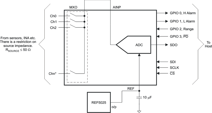
The ADS79xx device family offers 12/10/8-bit ADCSs with 16/12/8/4 channel multiplexers for analog input. The multiplexer output is available on the MXO pin. AINP is the ADC input pin. The devices offers flexibility for a system designer as both signals are accessible externally.
Typically it is convenient to short MXO to the AINP pin so that signal input to each multiplexer channel can be processed independently. In this condition, TI recommends limiting source impedance to 50 Ω or less. Higher source impedance may affect the signal settling time after a multiplexer channel change. This condition can affect linearity and total harmonic distortion.

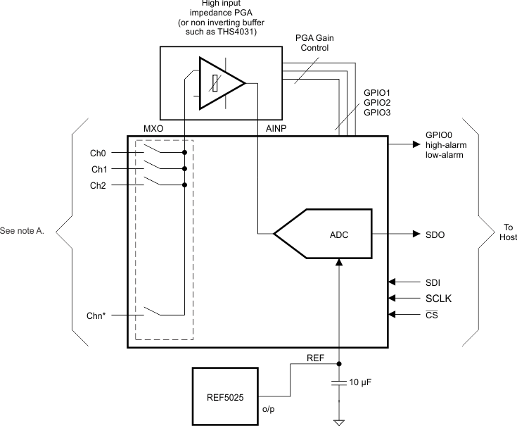
Another option is to add a common ADC driver buffer between the MXO and AINP pins. This relaxes the restriction on source impedance to a large extent. Refer to Typical Characteristics (All ADS79xx Family Devices) for the effect of source impedance on device performance. The typical characteristics show that the device has respectable performance with up to 1kΩ source impedance. This topology (including a common ADC driver) is useful when all channel signals are within the acceptable range of the ADC. In this case the user can save on signal conditioning circuit for each channel.
 Figure 61. Typical Application Diagram Showing Common Buffer/PGA for All Channels
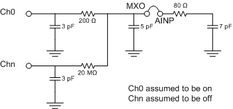
 When the converter samples an input, the voltage difference between AINP and AGND is captured on the internal capacitor array. The (peak) input current through the analog inputs depends upon a number of factors: sample rate, input voltage, and source impedance. The current into the ADS79xx charges the internal capacitor array during the sample period. After this capacitance has been fully charged, there is no further input current. When the converter goes into hold mode, the input impedance is greater than 1 GΩ.
Care must be taken regarding the absolute analog input voltage. To maintain linearity of the converter, the Ch0 .. Chn and AINP inputs should be within the limits specified. Outside of these ranges, converter linearity may not meet specifications.
 Figure 62. ADC and MUX Equivalent Circuit