JAJSFU8D November 2017 – June 2024 ADS8166 , ADS8167 , ADS8168
PRODUCTION DATA
- 1
- 1 特長
- 2 アプリケーション
- 3 概要
- 4 Pin Configuration and Functions
- 5 Specifications
- 6 Detailed Description
-
7 Register Maps
- 7.1
Interface and Hardware Configuration Registers
- 7.1.1 REG_ACCESS Register (address = 00h) [reset = 00h]
- 7.1.2 PD_CNTL Register (address = 04h) [reset = 00h]
- 7.1.3 SDI_CNTL Register (address = 008h) [reset = 00h]
- 7.1.4 SDO_CNTL1 Register (address = 0Ch) [reset = 00h]
- 7.1.5 SDO_CNTL2 Register (address = 0Dh) [reset = 00h]
- 7.1.6 SDO_CNTL3 Register (address = 0Eh) [reset = 00h]
- 7.1.7 SDO_CNTL4 Register (address = 0Fh) [reset = 00h]
- 7.1.8 DATA_CNTL Register (address = 10h) [reset = 00h]
- 7.1.9 PARITY_CNTL Register (address = 11h) [reset = 00h]
- 7.2 Device Calibration Registers
- 7.3 Analog Input Configuration Registers
- 7.4
Channel Sequence Configuration Registers Map
- 7.4.1 DEVICE_CFG Register (address = 1Ch) [reset = 00h]
- 7.4.2 CHANNEL_ID Register (address = 1Dh) [reset = 00h]
- 7.4.3 SEQ_START Register (address = 1Eh) [reset = 00h]
- 7.4.4 SEQ_ABORT Register (address = 1Fh) [reset = 00h]
- 7.4.5 ON_THE_FLY_CFG Register (address = 2Ah) [reset = 00h]
- 7.4.6 AUTO_SEQ_CFG1 Register (address = 80h) [reset = 00h]
- 7.4.7 AUTO_SEQ_CFG2 Register (address = 82h) [reset = 00h]
- 7.4.8
Custom Channel Sequencing Mode Registers
- 7.4.8.1 CCS_START_INDEX Register (address = 88h) [reset = 00h]
- 7.4.8.2 CCS_END_INDEX Register (address = 89h) [reset = 00h]
- 7.4.8.3 CCS_SEQ_LOOP Register (address = 8Ah) [reset = 00h]
- 7.4.8.4 CCS_CHID_INDEX_m Registers (address = 8C, 8E, 90, 92, 94, 96, 98, 9A, 9C, 9E, A0, A2, A4, A6, A8, and AAh) [reset = 00h]
- 7.4.8.5 REPEAT_INDEX_m Registers (address = 8D, 8F, 91, 93, 95, 97, 99, 9B, 9D, 9F, A1, A3, A5, A7, A9, and ABh) [reset = 00h]
- 7.5
Digital Window Comparator Configuration Registers Map
- 7.5.1 ALERT_CFG Register (address = 2Eh) [reset = 00h]
- 7.5.2 HI_TRIG_AINx[15:0] Register (address = 4Dh to 30h) [reset = 0000h]
- 7.5.3 LO_TRIG_AINx[15:0] Register (address = 71h to 54h) [reset = 0000h]
- 7.5.4 HYSTERESIS_AINx[7:0] Register (address = 4Fh to 33h) [reset = 00h]
- 7.5.5 ALERT_LO_STATUS Register (address = 78h) [reset = 00h]
- 7.5.6 ALERT_HI_STATUS Register (address = 79h) [reset = 00h]
- 7.5.7 ALERT_STATUS Register (address = 7Ah) [reset = 00h]
- 7.5.8 CURR_ALERT_LO_STATUS Register (address = 7Ch) [reset = 00h]
- 7.5.9 CURR_ALERT_HI_STATUS Register (address = 7Dh) [reset = 00h]
- 7.5.10 CURR_ALERT_STATUS Register (address = 7Eh) [reset = 00h]
- 7.1
Interface and Hardware Configuration Registers
- 8 Application and Implementation
- 9 Device and Documentation Support
- 10Revision History
- 11Mechanical, Packaging, and Orderable Information
パッケージ・オプション
メカニカル・データ(パッケージ|ピン)
- RHB|32
サーマルパッド・メカニカル・データ
- RHB|32
発注情報
6.3.2 Reference
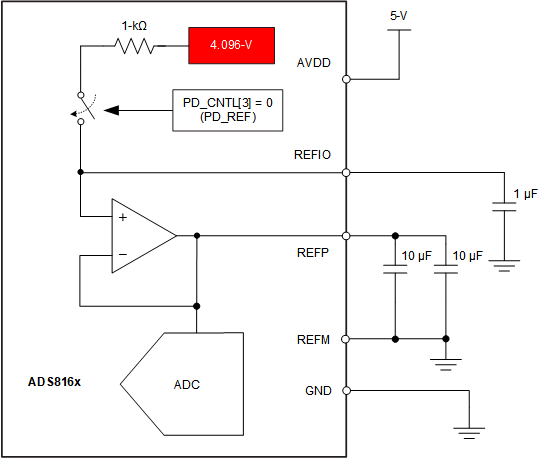
The ADS816x has a precision, low-drift reference internal to the device. The device features an internal reference source with a nominal output value of 4.096V. On power-up, the internal reference is enabled by default. Place a minimum 1µF decoupling capacitor, as illustrated in Figure 6-6, between the REFIO and REFM pins.
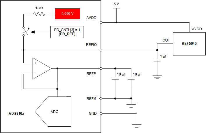
Figure 6-7 shows the connections for using the device with an external reference. Use a reference without a low-impedance output buffer because the input leakage current of the internal reference buffer is less than 1μA.
For the minimum ADC input offset error (VOS), set the REF_SEL[2:0] bits to the value closest to VREF (see the OFST_CAL register). Set the REF_OFST[4:0] (see the REF_MRG1 register) bits to add or subtract an intentional offset voltage as described in Table 7-14. Short the two REFP pins externally. Short the REFM pin to GND externally. Place a decoupling capacitor CREFP between the REFP and the REFM pins as close to the device as possible; see the Layout section for layout recommendations.
 Figure 6-6 Internal
Reference
 Figure 6-7 External
Reference