JAJSEC1C November   2019  – July 2020 ADS8686S

PRODUCTION DATA  

  1. 特長
  2. アプリケーション
  3. 概要
  4. Revision History
  5. Pin Configuration and Functions
  6. Specifications
    1. 6.1  Absolute Maximum Ratings
    2. 6.2  ESD Ratings
    3. 6.3  Recommended Operating Conditions
    4. 6.4  Thermal Information
    5. 6.5  Electrical Characteristics
    6. 6.6  Timing Requirements
    7. 6.7  Switching Characteristics
    8. 6.8  Timing Diagrams: Universal
    9. 6.9  Timing Diagrams: Parallel Data Read
    10. 6.10 Timing Diagrams: Serial Data Read
    11. 6.11 Typical Characteristics
  7. Detailed Description
    1. 7.1 Overview
    2. 7.2 Functional Block Diagram
    3. 7.3 Feature Description
      1. 7.3.1  Analog Inputs
      2. 7.3.2  Analog Input Impedance
      3. 7.3.3  Input Clamp Protection Circuit
      4. 7.3.4  Programmable Gain Amplifier (PGA)
      5. 7.3.5  Second-Order, Programmable, Low-Pass Filter (LPF)
      6. 7.3.6  ADC Driver
      7. 7.3.7  Multiplexer
      8. 7.3.8  Digital Filter and Noise
      9. 7.3.9  Reference
        1. 7.3.9.1 Internal Reference
        2. 7.3.9.2 External Reference
        3. 7.3.9.3 Supplying One VREF to Multiple Devices
      10. 7.3.10 ADC Transfer Function
    4. 7.4 Device Functional Modes
      1. 7.4.1 Device Interface: Pin Description
        1. 7.4.1.1  REFSEL (Input)
        2. 7.4.1.2  RESET (Input)
        3. 7.4.1.3  SEQEN (Input)
        4. 7.4.1.4  HW_RANGESEL[1:0] (Input)
        5. 7.4.1.5  SER/BYTE/PAR (Input)
        6. 7.4.1.6  DB[3:0] (Input/Output)
        7. 7.4.1.7  DB4/SER1W (Input/Output)
        8. 7.4.1.8  DB5/CRCEN (Input/Output)
        9. 7.4.1.9  DB[7:6] (Input/Output)
        10. 7.4.1.10 DB8 (Input/Output)
        11. 7.4.1.11 DB9/BYTESEL (Input/Output)
        12. 7.4.1.12 DB10/SDI (Input/Output)
        13. 7.4.1.13 DB11/SDOB (Input/Output)
        14. 7.4.1.14 DB12/SDOA (Input/Output)
        15. 7.4.1.15 DB13/OS0 (Input/Output)
        16. 7.4.1.16 DB14/OS1 (Input/Output)
        17. 7.4.1.17 DB15/OS2 (Input/Output)
        18. 7.4.1.18 WR/BURST (Input)
        19. 7.4.1.19 SCLK/RD (Input)
        20. 7.4.1.20 CS (Input)
        21. 7.4.1.21 CHSEL[2:0] (Input)
        22. 7.4.1.22 BUSY (Output)
        23. 7.4.1.23 CONVST (Input)
      2. 7.4.2 Device Modes of Operation
        1. 7.4.2.1 Shutdown Mode
        2. 7.4.2.2 Operation Mode
          1. 7.4.2.2.1 Hardware Mode
          2. 7.4.2.2.2 Software Mode
        3. 7.4.2.3 Reset Functionality
        4. 7.4.2.4 Channel Selection
          1. 7.4.2.4.1 Hardware Mode Channel Selection
          2. 7.4.2.4.2 Software Mode Channel Selection
        5. 7.4.2.5 Sequencer
          1. 7.4.2.5.1 Hardware Mode Sequencer
          2. 7.4.2.5.2 Software Mode Sequencer
        6. 7.4.2.6 Burst Sequencer
          1. 7.4.2.6.1 Hardware Mode Burst Sequencer
          2. 7.4.2.6.2 Software Mode Burst Sequencer
        7. 7.4.2.7 Diagnostics
          1. 7.4.2.7.1 Analog Diagnosis
          2. 7.4.2.7.2 Interface Diagnosis: SELF TEST and CRC
    5. 7.5 Programming
      1. 7.5.1 Parallel Interface
        1. 7.5.1.1 Reading Conversion Results
        2. 7.5.1.2 Writing Register Data
        3. 7.5.1.3 Reading Register Data
      2. 7.5.2 Parallel Byte Interface
        1. 7.5.2.1 Reading Conversion Results
        2. 7.5.2.2 Writing Register Data
        3. 7.5.2.3 Reading Register Data
      3. 7.5.3 Serial Interface
        1. 7.5.3.1 Reading Conversion Results
        2. 7.5.3.2 Writing Register Data
        3. 7.5.3.3 Reading Register Data
    6. 7.6 Register Maps
      1. 7.6.1 Page1 Registers
  8. Application and Implementation
    1. 8.1 Application Information
    2. 8.2 Typical Applications
      1. 8.2.1 8x2 Channel Data Acquisition System (DAQ) for Power Automation
        1. 8.2.1.1 Design Requirements
        2. 8.2.1.2 Detailed Design Procedure
        3. 8.2.1.3 Application Curve
      2. 8.2.2 Input Protection for Electrical Overstress
  9. Power Supply Recommendations
    1. 9.1 Power Supplies
  10. 10Layout
    1. 10.1 Layout Guidelines
    2. 10.2 Layout Examples
  11. 11Device and Documentation Support
    1. 11.1 Device Support
      1. 11.1.1 Development Support
    2. 11.2 Documentation Support
      1. 11.2.1 Related Documentation
    3. 11.3 Receiving Notification of Documentation Updates
    4. 11.4 サポート・リソース
    5. 11.5 Trademarks
    6. 11.6 Electrostatic Discharge Caution
    7. 11.7 Glossary

パッケージ・オプション

メカニカル・データ(パッケージ|ピン)
サーマルパッド・メカニカル・データ
発注情報
Hardware Mode Burst Sequencer

In hardware mode, set both the BURST and SEQEN pins to logic high to enable burst sequencer mode. The device latches these inputs when the RESET signal transitions from logic low to high after a full reset event. To exit the burst mode of operation, a full reset is needed.

When the burst sequencer is enabled, the logic levels of the CHSEL[2:0] pins determine the channels selected for the conversion in the burst sequence. The CHSEL[2:0] pins at the time that RESET is released determines the initial settings for the channels to convert in the burst sequence. To reconfigure the channels selected for conversion after a reset, set the CHSEL[2:0] pins to the required setting for the duration of the next BUSY pulse. Figure 7-18 shows a timing diagram of this mode.
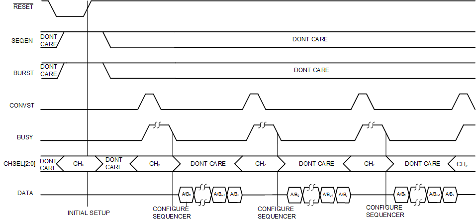
GUID-C322C8D5-65BA-4D8A-AEB5-DC5FC1DB08E1-low.gifFigure 7-18 Burst Sequencer, Hardware Mode