JAJSCN8A November 2016 – June 2017 ADS8900B , ADS8902B , ADS8904B
PRODUCTION DATA.
- 1 特長
- 2 アプリケーション
- 3 概要
- 4 改訂履歴
- 5 Pin Configuration and Functions
- 6 Specifications
-
7 Detailed Description
- 7.1 Overview
- 7.2 Functional Block Diagram
- 7.3 Feature Description
- 7.4 Device Functional Modes
- 7.5
Programming
- 7.5.1 Output Data Word
- 7.5.2 Data Transfer Frame
- 7.5.3 Interleaving Conversion Cycles and Data Transfer Frames
- 7.5.4 Data Transfer Protocols
- 7.5.5 Device Setup
- 7.6
Register Maps
- 7.6.1
Device Configuration and Register Maps
- 7.6.1.1 PD_CNTL Register (address = 04h) [reset = 00h]
- 7.6.1.2 SDI_CNTL Register (address = 008h) [reset = 00h]
- 7.6.1.3 SDO_CNTL Register (address = 0Ch) [reset = 00h]
- 7.6.1.4 DATA_CNTL Register (address = 010h) [reset = 00h]
- 7.6.1.5 PATN_LSB Register (address = 014h) [reset = 00h]
- 7.6.1.6 PATN_MID Register (address = 015h) [reset = 00h]
- 7.6.1.7 PATN_MSB Register (address = 016h) [reset = 00h]
- 7.6.1.8 OFST_CAL Register (address = 020h) [reset = 00h]
- 7.6.1.9 REF_MRG Register (address = 030h) [reset = 00h]
- 7.6.1
Device Configuration and Register Maps
-
8 Application and Implementation
- 8.1 Application Information
- 8.2 Typical Application
- 9 Power-Supply Recommendations
- 10Layout
- 11デバイスおよびドキュメントのサポート
- 12メカニカル、パッケージ、および注文情報
パッケージ・オプション
メカニカル・データ(パッケージ|ピン)
- RGE|24
サーマルパッド・メカニカル・データ
- RGE|24
発注情報
7 Detailed Description
7.1 Overview
The ADS890xB is a family of high-speed, successive approximation register (SAR), analog-to-digital converters (ADC) based on a charge redistribution architecture. These compact devices integrate a reference buffer and LDO, and feature high performance at a high throughput rate with low power consumption.
This device family supports unipolar, fully differential, analog input signals. The integrated reference buffer supports the burst mode of data acquisition for external reference voltages in the range 2.5 V to 5 V, and offers a wide selection of input ranges without additional input scaling.
When a conversion is initiated, the differential input between the AINP and AINM pins is sampled on the internal capacitor array. The device uses an internal clock to perform conversions. During the conversion process, both analog inputs are disconnected from the internal circuit. At the end of conversion process, the device reconnects the sampling capacitors to the AINP and AINM pins and enters an acquisition phase.
The integrated LDO allows the device to operate on a single supply, RVDD. The device consumes only 21 mW, 16 mW, or 14 mW of power when operating at the rated maximum throughput of 1 MSPS, 500 kSPS, or 250 kSPS, respectively, with the internal reference buffer and LDO enabled.
The enhanced multiSPI digital interface is backward-compatible with traditional SPI protocol. Configurable features simplify board layout, timing, and firmware, and support high throughput at lower clock speeds, thus allowing an easy interface with a variety of microcontrollers, DSPs, and FPGAs.
The ADS890xB enables test and measurement, medical, and industrial applications to achieve fast, low-noise, low-distortion, low-power data acquisition in small form factors.
7.2 Functional Block Diagram

7.3 Feature Description
From a functional perspective, the device comprises four modules: the low-dropout regulator (LDO), the reference buffer (BUF), the converter (SAR ADC), and the interface (multiSPI digital interface), as shown in the Functional Block Diagram section.
The LDO module is powered by the RVDD supply, and generates the bias voltage for internal circuit blocks of the device. The reference buffer module buffers the external reference voltage source from the dynamic, capacitive switching load present on the reference pins during the conversion process. The converter module samples and converts the analog input into an equivalent digital output code. The interface module facilitates communication and data transfer between the device and the host controller.
7.3.1 LDO Module
To enable single-supply operation, the device features an internal low-dropout regulator (LDO). The LDO is powered by the RVDD supply, and the output is available on the two DECAP pins. This LDO output powers the critical analog blocks within the device, and must not be used for any other external purposes.
Short the two DECAP pins together, and decouple with the GND pin by placing a 1-μF, X7R-grade, ceramic capacitor with a 10-V rating, as shown in Figure 32. There is no upper limit on the value of the decoupling capacitor; however, a larger decoupling capacitor results in a longer power-up time for the device. See the Layout section for layout recommendations.
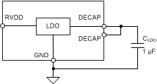 Figure 32. Internal LDO Connections
7.3.2 Reference Buffer Module
On the CONVST rising edge, the device moves from ACQ state to CONV state, and the internal capacitors are switched to the REFBUFOUT pins as per the successive approximation algorithm. Most of the switching charge required during the conversion process is provided by external decoupling capacitor CREFBUF. If the charge lost from the CREFBUF is not replenished before the next CONVST rising edge, the voltage on REFBUFOUT pins is less than VREFBUFOUT. The subsequent conversion occurs with this different reference voltage, and causes a proportional error in the output code. The internal reference buffer of the device maintains the voltage on REFBUFOUT pins within 0.5-LSB of VREFBUFOUT. All the performance characteristics of the device are specified with the internal reference buffer and specified values of CREFBUF and RESR.
In burst-mode of operation, the device stays in ACQ state for a long duration of time and then performs a burst of conversions. During the acquisition state (ACQ), the sampling capacitor (CS) is connected to the differential input pins and no charge is drawn from the REFBUFOUT pins. However, during the very first conversion cycle, there is a step change in the current drawn from the REFBUFOUT pins. This sudden change in load triggers a transient settling response in the reference buffer. For a fixed input voltage, any transient settling error at the end of the conversion cycle results in a change in output codes over the subsequent conversions, as shown in Figure 33. The internal reference buffer of the ADS89xxB, when used with the recommended values of CREFBUF and RESR, keeps the transient settling error at the end of each conversion cycle within 0.5-LSB. Therefore, the device supports burst-mode of operation with every conversion result being as per the datasheet specifications.
 Figure 33. ADC Output Codes in Burst-Mode Operation With Various ADC Reference Buffers
Figure 34 shows the block diagram of the internal reference buffer.
 Figure 34. Internal Reference Buffer Block Diagram
The input range for the device is set by the external voltage applied at the REFIN pin (VREF). The REFIN pin has electrostatic discharge (ESD) protection diodes to the RVDD and GND pins. For minimum input offset error (see E(IO) specified in the Electrical Characteristics), set the REF_SEL[2:0] bits to the value closest to VREF (see the OFST_CAL register).
The internal reference buffer has a typical gain of 1 V/V with minimal offset error (see V(RO) specified in the Electrical Characteristics), and the output of the buffer is available between the REFBUFOUT pins and the REFM pins. Set the REF_OFST[4:0] bits to add or subtract an intentional offset voltage (see the REF_MRG register).
Figure 35 shows the external connections required for the internal reference buffer.
 Figure 35. External Connections for the Internal Reference Buffer
Select RREF_FLT and CREF_FLT to limit the broadband noise contribution from the external reference source. The device takes very little current, IREF, from the REFIN pin (typically, 0.1 µA). However, this current flows through RREF_FLT and may result in additional gain error.
Short the two REFBUFOUT pins externally. Short the two REFM pins to GND externally. As shown in Figure 35, place a combination of RESR and CREFBUF (see the Electrical Characteristics) between the REFBUFOUT pins and the REFM pins as close to the device as possible. See the Layout section for layout recommendations.
7.3.3 Converter Module
As shown in Figure 36, the converter module samples the analog input signal (provided between the AINP and AINM pins), compares this signal with the reference voltage (between the pair of REFBUFOUT and REFM pins), and generates an equivalent digital output code.
The converter module receives RST and CONVST inputs from the interface module, and outputs the ADCST signal and the conversion result back to the interface module.
 Figure 36. Converter Module
7.3.3.1 Sample-and-Hold Circuit
These devices support unipolar, fully differential, analog input signals. Figure 37 shows a small-signal equivalent circuit of the sample-and-hold circuit. Each sampling switch is represented by a resistance (RS1 and RS2, typically 50 Ω) in series with an ideal switch (SW1 and SW2). The sampling capacitors, CS1 and CS2, are typically 60 pF.
 Figure 37. Input Sampling Stage Equivalent Circuit
During the acquisition process (ACQ state), both positive and negative inputs are individually sampled on CS1 and CS2, respectively. During the conversion process (CNV state), the device converts for the voltage difference between the two sampled values: VAINP – VAINM.
Each analog input pin has electrostatic discharge (ESD) protection diodes to REFBUFOUT and GND. Keep the analog inputs within the specified range to avoid turning the diodes on.
Equation 1 and Equation 2 show the full-scale input range (FSR) and common-mode voltage (VCM), respectively, supported at the analog inputs for any external reference voltage provided on the REFIN pin (VREF).


7.3.3.2 Internal Oscillator
The device family features an internal oscillator (OSC) that provides the conversion clock; see Figure 36. The conversion duration is bound by the minimum and maximum value of tconv, as specified in the Switching Characteristics table.
The interface module uses this internal clock (OSC), an external clock (provided by the host controller on the SCLK pin), or a combination of both the internal and external clocks, to execute the data transfer operations between the device and host controller; see the Interface Module section for more details.
7.3.3.3 ADC Transfer Function
The device family supports unipolar, fully differential analog inputs. The device output is in two's compliment format. Figure 38 and Table 1 show the ideal transfer characteristics for the device.
The least significant bit (LSB) for the ADC is given by Equation 3:

where
 Figure 38. Differential Transfer Characteristics
Table 1. Transfer Characteristics
| DIFFERENTIAL ANALOG INPUT VOLTAGE (AINP – AINM) |
OUTPUT CODE (HEX) |
|---|---|
| < –VREF | 80000 |
| –VREF + 1 LSB | 80001 |
| –1 LSB | FFFFF |
| 0 | 00000 |
| 1 LSB | 00001 |
| > VREF – 1 LSB | 7FFFF |
7.3.4 Interface Module
The interface module facilitates the communication and data transfer between the device and the host controller. As shown in Figure 39, the module consists of shift registers (both input and output), configuration registers, and a protocol unit.
 Figure 39. Interface Module
The Pin Configuration and Functions section provides descriptions of the interface pins. The Data Transfer Frame section details the functions of shift registers, the SCLK counter, and the command processor. The Data Transfer Protocols section details supported protocols. The Register Maps section explains the configuration registers and bit settings.
7.4 Device Functional Modes
As shown in Figure 40, this device family supports three functional states: RST, ACQ, and CNV. The device state is determined by the status of the CONVST and RST control signals provided by the host controller.
 Figure 40. Device Functional States
7.4.1 RST State
The RST pin is an asynchronous digital input for the device. To enter RST state, the host controller pulls the RST pin low and keeps it low for the twl_RST duration (as specified in the Timing Requirements table).
In RST state, all configuration registers (see the Register Maps section) are reset to their default values, the RVS pin remains low, and the SDO-x pins are Hi-Z.
To exit RST state, the host controller pulls the RST pin high, with CONVST and SCLK held low and CS held high, as shown in Figure 41. After a delay of td_rst, the device enters ACQ state and the RVS pin goes high.
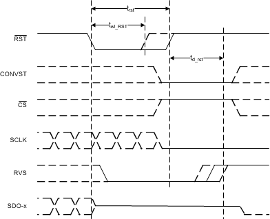 Figure 41. Asynchronous Reset
To operate the device in either ACQ or CNV state, RST must be held high. With RST held high, transitions on the CONVST pin determine the functional state of the device.
Figure 42 shows a typical conversion process. The internal ADCST signal goes low during conversion and goes high at the end of conversion. With CS held high, RVS reflects the status of ADCST.
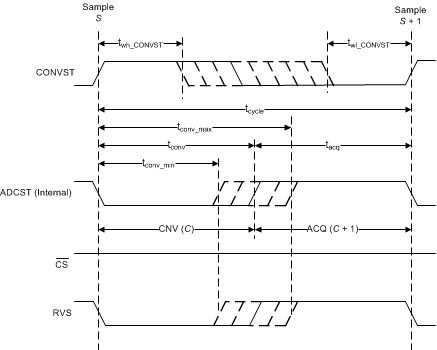 Figure 42. Typical Conversion Process
7.4.2 ACQ State
In ACQ state, the device acquires the analog input signal. The device enters ACQ state at power-up, when coming out of power down (See the PD Control section), after any asynchronous reset, and at the end of every conversion.
An RST falling edge takes the device from ACQ state to RST state. A CONVST rising edge takes the device from ACQ state to CNV state.
7.4.3 CNV State
The device moves from ACQ state to CNV state on a rising edge of the CONVST pin. The conversion process uses an internal clock. The device ignores any further transitions on the CONVST signal until the ongoing conversion is complete (that is, during the time interval of tconv).
At the end of conversion, the device enters ACQ state. The cycle time for the device is given by Equation 4:

NOTE
The conversion time, tconv, varies within the specified limits of tconv_min and tconv_max (as specified in the Switching Characteristics table). After initiating a conversion, the host controller must monitor for a low-to-high transition on the RVS pin or wait for the tconv_max duration to elapse before initiating a new operation (data transfer or conversion). If RVS is not monitored, substitute tconv in Equation 4 with tconv_max.
7.5 Programming
This device family features nine configuration registers (as described in the Register Maps section). To access the internal configuration registers, these devices support the commands listed in Table 2.
Table 2. Supported Commands
| B[21:17] | B[16:8] | B[7:0] | COMMAND ACRONYM | COMMAND DESCRIPTION |
|---|---|---|---|---|
| 00000 | 000000000 | 00000000 | NOP | No operation |
| 10000 | <9-bit address> | <8-bit unmasked bits> | CLR_BITS | Clear <8-bit unmasked bits> from <9-bit address> |
| 10001 | <9-bit address> | 00000000 | RD_REG | Read contents from the <9-bit address> |
| 10010 | <9-bit address> | <8-bit data> | WR_REG | Write <8-bit data> to the <9-bit address> |
| 10011 | <9-bit address> | <8-bit unmasked bits> | SET_BITS | Set <8-bit unmasked bits> from <9-bit address> |
| 11111 | 111111111 | 11111111 | NOP | No operation |
| Remaining combinations | xxxxxxxxx | xxxxxxxx | Reserved | These commands are reserved and treated by the device as no operation |
These devices support two types of data transfer operations: data write (the host controller configures the device), and data read (the host controller reads data from the device).
Any data write to the device is always synchronous to the external clock provided on the SCLK pin. The WR_REG command writes the 8-bit data into the 9-bit address specified in the command string. The CLR_BITS command clears the specified bits (identified by 1) at the 9-bit address (without affecting the other bits), and the SET_BITS command sets the specified bits (identified by 1) at the 9-bit address (without affecting the other bits).
The data read from the device can be synchronized to the same external clock or to an internal clock of the device by programming the configuration registers (see the Data Transfer Protocols section for details).
7.5.1 Output Data Word
In any data transfer frame, the contents of an internal, 22-bit, output data word are shifted out on the SDO pins. The D[21:2] bits of the 22-bit output data word for any frame F + 1, are determined by:
- Value of the DATA_VAL bit applicable to frame F + 1 (see the DATA_CNTL register)
- The command issued in frame F
If a valid RD_REG command is executed in frame F, then the D[21:14] bits in frame F + 1 reflect the contents of the selected register, and the D[13:0] bits are zeros.
If the DATA_VAL bit for frame F + 1 is set to 1, then the D[21:2] bits in frame F + 1 are replaced by the DATA_PATN[19:0] bits.
For all other combinations, the D[21:2] bits for frame F + 1 are the latest conversion result.
Figure 43 shows the output data word. Figure 44 shows further details of the parity computation unit illustrated in Figure 43.
![ADS8900B ADS8902B ADS8904B Output Data Word
(D[21:0]) ADS8900B ADS8902B ADS8904B ai_odw_config_20_bas707.gif](/ods/images/JAJSCN8A/ai_odw_config_20_bas707.gif) Figure 43. Output Data Word (D[21:0])
Figure 43. Output Data Word (D[21:0])
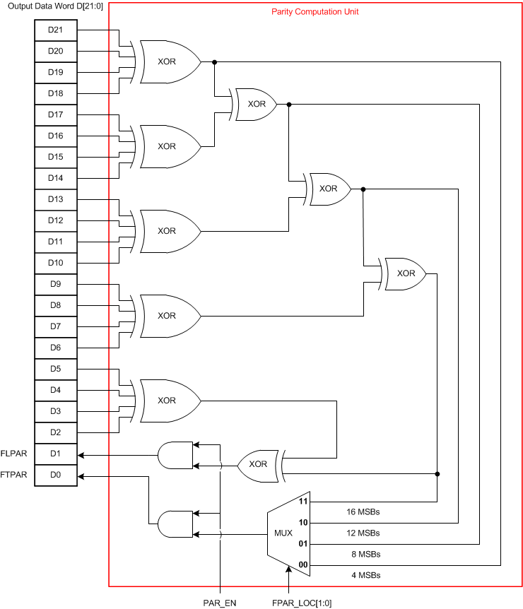 Figure 44. Parity Bits Computation
With the PAR_EN bit set to 0, the D[1] and D[0] bits of the output data word are set to 0 (default configuration).
When the PAR_EN bit is set to 1, the device calculates the parity bits (FLPAR and FTPAR) and appends them as bits D[1] and D[0].
- FLPAR is the even parity calculated on bits D[21:2].
- FTPAR is the even parity calculated on the bits defined by FPAR_LOC[1:0].
See the DATA_CNTL register for more details on the FPAR_LOC[1:0] bit settings.
7.5.2 Data Transfer Frame
A data transfer frame between the device and the host controller is bounded between a CS falling edge and the subsequent CS rising edge. The host controller can initiate a data transfer frame (as shown in Figure 45) at any time irrespective of the status of the CONVST signal; however, the data read during such a data transfer frame is a function of relative timing between the CONVST and CS signals.
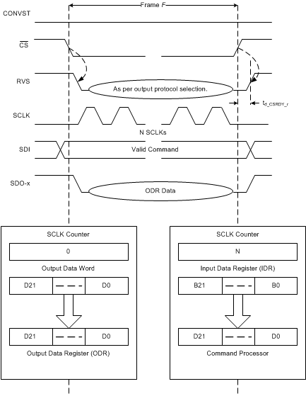 Figure 45. Data Transfer Frame
For this discussion, assume that the CONVST signal remains low.
A typical data transfer frame F follows this order:
- The host controller pulls CS low to initiate a data transfer frame. On the CS falling edge:
- RVS goes low, indicating the beginning of the data transfer frame.
- The SCLK counter is reset to 0.
- The device takes control of the data bus. As shown in Figure 45, the 22-bit contents of the output data word (see Figure 43) are loaded in to the 22-bit output data register (ODR; see Figure 39).
- The 22-bit input data register (IDR; see Figure 39) is reset to 000000h, corresponding to a NOP command.
- During the frame, the host controller provides clocks on the SCLK pin. Inside the device:
- For each SCLK capture edge, the SCLK counter is incremented and the data bit received on the SDI pin is shifted in to the IDR.
- For each launch edge of the output clock (SCLK in this case), ODR data are shifted out on the selected SDO-x pins.
- The status of the RVS pin depends on the output protocol selection (see the Protocols for Reading From the Device section).
- The host controller pulls CS high to end the data transfer frame. On the CS rising edge:
After pulling CS high, the host controller monitors for a low-to-high transition on the RVS pin, or waits for the td_CSRDY_r time (see the Switching Characteristics table) to elapse before initiating a new operation (data transfer or conversion). The delay, td_CSRDY_r, for any data transfer frame F varies based on the data transfer operation executed in frame F.
At the end of data transfer frame F:
- If the SCLK counter is < 22, then the IDR captured less than 22 bits from the SDI. In this case, the device treats frame F as a short command frame. At the end of a short command frame, the IDR is not updated and the device treats the frame as a no operation (NOP) command.
- If the SCLK counter = 22, then the IDR captured exactly 22 bits from SDI. In this case, the device treats the frame F as a optimal command frame. At the end of an optimal command frame, the command processor decodes the 22-bit contents of the IDR as a valid command word.
- If the SCLK counter > 22, then the IDR captured more than 22 bits from the SDI; however, only the last 22 bits are retained. In this case, the device treats frame F as a long command frame. At the end of a long command frame, the command processor treats the 22-bit contents of the IDR as a valid command word. There is no restriction on the maximum number of clocks that can be provided within any data transfer frame F. However, as explained above, make sure that the last 22 bits shifted into the device before the CS rising edge constitute the desired command.
In a short command frame, the write operation to the device is invalidated; however, the output data bits transferred during the short command frame are still valid output data. Therefore, the host controller can use such shorter data transfer frames to read only the required number of MSB bits from the 22-bit output data word. As shown in Figure 43, an optimal read frame for the ADS890xB devices must read only the 20 MSB bits of the output data word. The length of an optimal read frame depends on the output protocol selection; see the Protocols for Reading From the Device section for more details.
NOTE
The previous example shows data-read and data-write operations synchronous to the external clock provided on the SCLK pin.
However, the device also supports data read operation synchronous to the internal clock; see the Protocols for Reading From the Device section for more details. In this case, while the ODR contents are shifted on the SDO (or SDOs) on the launch edge of the internal clock, the device continues to capture the SDI data into the IDR (and increment the SCLK counter) on SCLK capture edges.
7.5.3 Interleaving Conversion Cycles and Data Transfer Frames
The host controller operates the device at the desired throughput by interleaving the conversion cycles and the data transfer frames.
The cycle time of the device, tcycle, is the time difference between two consecutive CONVST rising edges provided by the host controller. The response time of the device, tresp, is the time difference between the host controller initiating conversion C, and the host controller receiving the complete result for conversion C.
Figure 46 shows three conversion cycles: C, C + 1, and C + 2. Conversion C is initiated by a CONVST rising edge at time t = 0, and the conversion result becomes available for data transfer at tconv. However, this result is loaded into the ODR only on the subsequent CS falling edge. This CS falling edge must be provided before the completion of conversion C + 1 (that is, before tcycle + tconv).
To achieve the rated performance specifications, the host controller must make sure that no digital signals toggle during the quiet acquisition time (tqt_acq) and quiet aperture time (td_cnvcap). Any noise during td_cnvcap may negatively affect the result of the ongoing conversion, whereas any noise during tqt_acq may negatively affect the result of the subsequent conversion.
 Figure 46. Data Transfer Zones
This architecture allows for two distinct time zones (zone 1 and zone 2) to transfer data for each conversion. Zone 1 and zone 2 for conversion C are defined in Table 3.
Table 3. Data Transfer Zones Timing
| ZONE | STARTING TIME | ENDING TIME |
|---|---|---|
| Zone 1 for conversion C |  |
 |
| Zone 2 for conversion C |  |
 |
The response time includes the conversion time and the data transfer time, and thus is a function of the selected data transfer zone.
Figure 47 and Figure 48 illustrate interleaving of three conversion cycles (C, C + 1, and C + 2) with three data transfer frames (F, F + 1, and F + 2) in zone 1 and in zone 2, respectively.
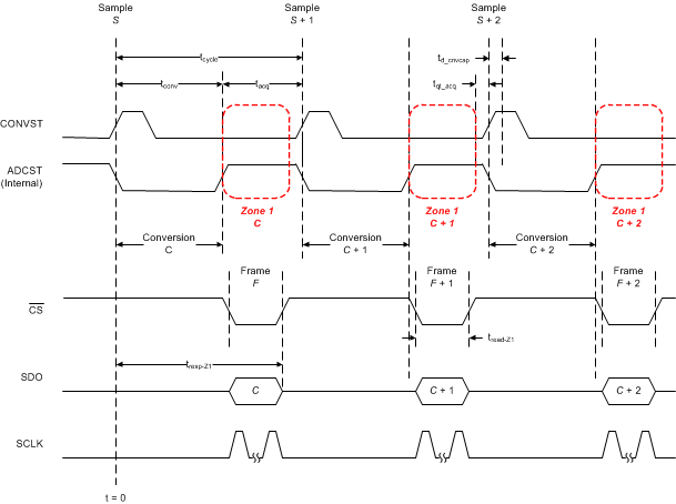 Figure 47. Zone 1 Data Transfer
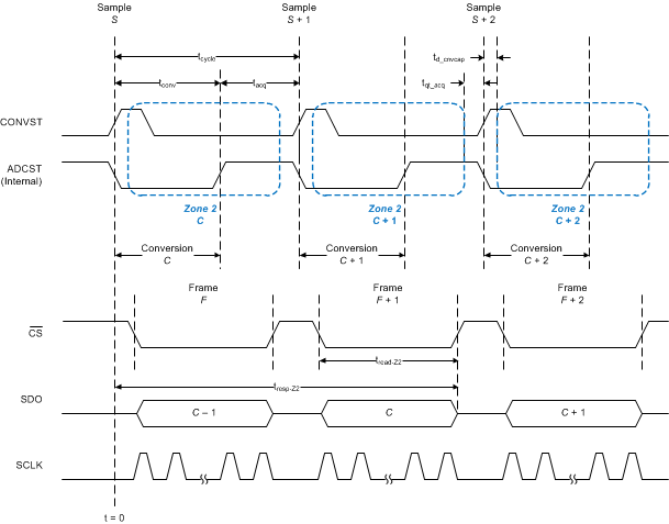 Figure 48. Zone 2 Data Transfer
To achieve cycle time tcycle, the read time in zone 1 is given by Equation 5:

For an optimal data transfer frame, Equation 5 results in an SCLK frequency given by Equation 6:

Then, the zone 1 data transfer achieves a response time defined by Equation 7:

At lower SCLK speeds, tread-Z1 increases, resulting in slower response times and higher cycle times.
To achieve the same cycle time, tcycle, the read time in zone 2 is given by Equation 8:

For an optimal data transfer frame, Equation 8 results in an SCLK frequency given by Equation 9:

Then, the zone 2 data transfer achieves a response time defined by Equation 10:

Any increase in tread-Z2 increases response time and may increase cycle time.
For a given cycle time, the zone 1 data transfer clearly achieves faster response time, but also requires a higher SCLK speed (as evident from Equation 5, Equation 6, and Equation 7); whereas, the zone 2 data transfer clearly requires a lower SCLK speed but has a slower response time (as evident from Equation 8, Equation 9, and Equation 10).
NOTE
A data transfer frame can begin in zone 1, and then extend into zone 2; however, the host controller must make sure that no digital transitions occur during the tqt_acq and td_cnvcap time intervals.
NOTE
For data transfer operations in zone 2 using the ADC-Clock-Master protocol
(SDO_MODE[1:0] = 11b), the device supports only the external-clock-echo option
(SSYNC_CLK_SEL[1:0] = 00b); see Table 9.
7.5.4 Data Transfer Protocols
This device family features a multiSPI digital interface that allows the host controller to operate at slower SCLK speeds and still achieve the required throughput and response time. The multiSPI digital interface module offers three options to reduce the SCLK speed required for data transfer:
- Increase the width of the output data bus.
- Enable double data rate (DDR) transfer.
- Extended data transfer window, as shown in Figure 48.
These three options can be combined to achieve further reduction in SCLK speed.
There are various factors that limit the maximum SCLK frequency in a system.
Figure 49 shows the delays in the communication channel between the host controller and the device in a typical serial communication.
 Figure 49. Delays in Serial Communication
For example, if tpcb_CK and tpcb_SDO are the delays introduced by the printed circuit board (PCB) traces for the serial clock and SDO signals, td_CKDO is the clock-to-data delay of the device, td_ISO is the propagation delay introduced by the digital isolator, and tsu_h is the setup time specification of the host controller, then the total delay in the path is given by Equation 11:

In a standard SPI protocol, the host controller and the device launch and capture data bits on alternate SCLK edges. Therefore, the td_total_serial delay must be kept to less than half of the SCLK duration. Equation 12 shows the fastest clock allowed by the SPI protocol:

Larger values of the td_total_serial delay restricts the maximum SCLK speed for the SPI protocol, resulting in higher read and response times, and can possibly limit the throughput.
Figure 50 shows a delay (td_delcap) introduced in the capture path (inside the host controller).
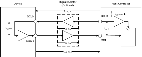 Figure 50. Delayed Capture
The total delay in the path modifies to Equation 13:

This reduction in total delay allows the SPI protocol to operate at higher clock speeds.
The multiSPI digital interface module offers two additional options to remove the restriction on the SCLK speed:
- Early data launch (EDL) mode of operation
- ADC-Clock-Master (source-synchronous) mode of operation
In EDL mode, the device launches the output data on SDO-x pin (or pins) half a clock earlier compared to the standard SPI protocol. Therefore, Equation 12 modifies to Equation 14:

The reduction in total delay allows the serial interface to operate at higher clock speeds.
As illustrated in Figure 51, in ADC-Clock-Master mode, the device provides a synchronous output clock (on the RVS pin) along with the output data (on the SDO-x pins).
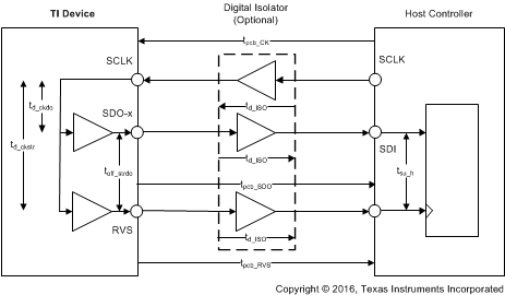 Figure 51. Delays in ADC-Clock-Master (Source-Synchronous) Mode
For negligible values of toff_STRDO, the total delay in the path for a source-synchronous data transfer, is given by Equation 15:

As shown by the difference between Equation 11 and Equation 15, using ADC-Clock-Master mode completely eliminates the effect of isolator delays (td_ISO) and clock-to-data delays (td_CKDO); typically, the largest contributors in the overall delay computation.
Furthermore, the actual values of tpcb_RVS and tpcb_SDO do not matter. In most cases, the td_total_srcsync delay can be kept at a minimum by routing the RVS and SDO lines together on the PCB. Therefore, the ADC-Clock-Master mode allows the data transfer between the host controller and the device to operate at much higher SCLK speeds.
7.5.4.1 Protocols for Configuring the Device
As shown in Table 4, the host controller can use any of the four legacy, SPI-compatible protocols (SPI-00-S, SPI-01-S, SPI-10-S, or SPI-11-S) to write data to the device.
Table 4. SPI Protocols for Configuring the Device
| PROTOCOL | SCLK POLARITY (At CS Falling Edge) |
SCLK PHASE (Capture Edge) |
SDI_CNTL | SDO_CNTL | NO. OF SCLK (Optimal Command Frame) |
TIMING DIAGRAM |
|---|---|---|---|---|---|---|
| SPI-00-S | Low | Rising | 00h | 00h | 22 | Figure 52 |
| SPI-01-S | Low | Falling | 01h | 00h | 22 | Figure 53 |
| SPI-10-S | High | Falling | 02h | 00h | 22 | Figure 54 |
| SPI-11-S | High | Rising | 03h | 00h | 22 | Figure 55 |
At power-up or after coming out of any asynchronous reset, the device supports the SPI-00-S protocol for data-read and data-write operations.
To select a different SPI-compatible protocol, program the SDI_MODE[1:0] bits in the SDI_CNTL register. This first write operation must adhere to the SPI-00-S protocol. Any subsequent data transfer frames must adhere to the newly selected protocol.
Figure 52 to Figure 55 detail the four protocols using an optimal command frame; see the Timing Requirements and Switching Characteristics tables for associated timing parameters.
NOTE
As explained in the Data Transfer Frame section, a valid write operation to the device requires a minimum of 22 SCLKs to be provided within a data transfer frame.
Any data write operation to the device must continue to follow the SPI-compatible protocol selected in the SDI_CNTL register, irrespective of the protocol selected for the data-read operation.
 Figure 52. SPI-00-S Protocol, Optimal Command Frame
 Figure 54. SPI-10-S Protocol, Optimal Command Frame
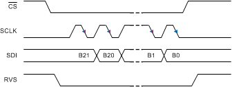 Figure 53. SPI-01-S Protocol, Optimal Command Frame
 Figure 55. SPI-11-S Protocol, Optimal Command Frame
7.5.4.2 Protocols for Reading From the Device
The protocols for the data-read operation can be broadly classified into three categories:
- Legacy, SPI-compatible (SPI-xy-S) protocol
- SPI-compatible protocols with bus width options (SPI-xy-D and SPI-xy-Q)
- Source-synchronous (SRC) protocols
7.5.4.2.1 Legacy, SPI-Compatible (SYS-xy-S) Protocols
As shown in Table 5, the host controller can use any of the four legacy, SPI-compatible protocols (SPI-00-S, SPI-01-S, SPI-10-S, or SPI-11-S) to read data from the device.
Table 5. SPI Protocols for Reading From the Device
| PROTOCOL | SCLK POLARITY (At CS Falling Edge) |
SCLK PHASE (Capture Edge) |
MSB BIT LAUNCH EDGE | SDI_CNTL | SDO_CNTL | NO. OF SCLK (Optimal Read Frame) |
TIMING DIAGRAM |
|---|---|---|---|---|---|---|---|
| SPI-00-S | Low | Rising | CS falling | 00h | 00h | 20 | Figure 56 |
| SPI-01-S | Low | Falling | 1st SCLK rising | 01h | 00h | 20 | Figure 57 |
| SPI-10-S | High | Falling | CS falling | 02h | 00h | 20 | Figure 58 |
| SPI-11-S | High | Rising | 1st SCLK falling | 03h | 00h | 20 | Figure 59 |
At power-up or after coming out of any asynchronous reset, the device supports the SPI-00-S protocol for data-read and data-write operations. To select a different SPI-compatible protocol for both the data transfer operations:
- Program the SDI_MODE[1:0] bits in the SDI_CNTL register. This first write operation must adhere to the SPI-00-S protocol. Any subsequent data transfer frames must adhere to the newly selected protocol.
- Set the SDO_MODE[1:0] bits = 00b in the SDO_CNTL register.
Figure 56 to Figure 59 explain the details of the four protocols using an optimal command frame to read all 22 bits of the output data word. Table 5 shows the number of SCLK required in an optimal read frame for the different output protocol selections.
 Figure 56. SPI-00-S Protocol, 22 SCLKs
 Figure 58. SPI-10-S Protocol, 22 SCLKs
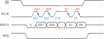 Figure 57. SPI-01-S Protocol, 22 SCLKs
 Figure 59. SPI-11-S Protocol, 22 SCLKs
For SDI_MODE[1:0] = 00b or 10b, the device supports an Early Data Launch (EDL) option. Set SDO_MODE[1:0] = 01b in the SDO_CNTL register to enable the feature (see Table 6). Setting SDO_MODE[1:0] = 01b has no effect if SDI_MODE[1:0] = 01b or 11b.
Table 6. SPI Protocols with Early Data Launch
| PROTOCOL | SCLK POLARITY (At CS Falling Edge) |
SCLK PHASE (Capture Edge) |
MSB BIT LAUNCH EDGE | SDI_CNTL | SDO_CNTL | NO. OF SCLK (Optimal Read Frame) |
TIMING DIAGRAM |
|---|---|---|---|---|---|---|---|
| SPI-00-S-EDL | Low | Rising | CS falling | 00h | 01h | 20 | Figure 56 |
| SPI-10-S-EDL | High | Falling | CS falling | 02h | 01h | 20 | Figure 58 |
As shown in Figure 60, and Figure 61, the device launches the output data bit on the SDO-0 pin half clock earlier compared to the standard SPI protocol.
 Figure 60. SPI-00-S-EDL Protocol, 22 SCLKs
 Figure 61. SPI-10-S-EDL Protocol, 22 SCLKs
When using these SPI-compatible protocols, the RVS output remains low throughout the data transfer frame; see the Timing Requirements and Switching Characteristics tables for associated timing parameters.
With SDO_CNTL[7:0] = 00h or 01h, if the host controller uses a long data transfer frame, the device exhibits daisy-chain operation (see the Multiple Devices: Daisy-Chain Topology section).
NOTE
Use SPI-compatible protocols to execute the RD_REG, WR_REG, CLR_BITS, and SET_BITS commands specified in Table 2.
7.5.4.2.2 SPI-Compatible Protocols with Bus Width Options
The device provides an option to increase the SDO bus width from one bit (default, single SDO) to two bits (dual SDO) or four bits (quad SDO) when operating with any of the four legacy, SPI-compatible protocols.
Set the SDO_WIDTH[1:0] bits in the SDO_CNTL register to select the SDO bus width. The SCLK launch edge depends on the SPI protocol selection (as shown in Table 7).
Table 7. SPI-Compatible Protocols with Bus Width Options
| PROTOCOL | SCLK POLARITY (At CS Falling Edge) |
SCLK PHASE (Capture Edge) |
MSB BIT LAUNCH EDGE | SDI_CNTL | SDO_CNTL | #SCLK (Optimal Read Frame) |
TIMING DIAGRAM |
|---|---|---|---|---|---|---|---|
| SPI-00-D | Low | Rising | CS falling | 00h | 08h | 10 | Figure 62 |
| SPI-01-D | Low | Falling | First SCLK rising | 01h | 08h | 10 | Figure 63 |
| SPI-10-D | High | Falling | CS falling | 02h | 08h | 10 | Figure 64 |
| SPI-11-D | High | Rising | First SCLK falling | 03h | 08h | 10 | Figure 65 |
| SPI-00-Q | Low | Rising | CS falling | 00h | 0Ch | 5 | Figure 66 |
| SPI-01-Q | Low | Falling | First SCLK rising | 01h | 0Ch | 5 | Figure 67 |
| SPI-10-Q | High | Falling | CS falling | 02h | 0Ch | 5 | Figure 68 |
| SPI-11-Q | High | Rising | First SCLK falling | 03h | 0Ch | 5 | Figure 69 |
In dual-SDO mode (SDO_WIDTH[1:0] = 10b), two bits of data are launched on the two SDO pins (SDO-0 and SDO-1) on every SCLK launch edge.
In quad-SDO mode (SDO_WIDTH[1:0] = 11b), four bits of data are launched on the four SDO pins (SDO-0, SDO-1, SDO-2, and SDO-3) on every SCLK launch edge.
 Figure 62. SPI-00-D Protocol
 Figure 64. SPI-10-D Protocol
 Figure 66. SPI-00-Q Protocol
 Figure 68. SPI-10-Q Protocol
 Figure 63. SPI-01-D Protocol
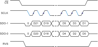 Figure 65. SPI-11-D Protocol
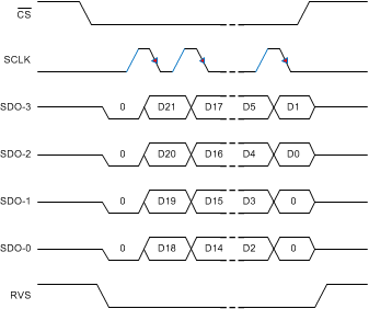 Figure 67. SPI-01-Q Protocol
 Figure 69. SPI-11-Q Protocol
For SDI_MODE[1:0] = 00b or 10b, the device supports an early data launch (EDL) option. Set SDO_MODE[1:0] = 01b in the SDO_CNTL register to enable the feature (see Table 8). Setting SDO_MODE[1:0] = 01b has no effect if SDI_MODE[1:0] = 01b or 11b.
Table 8. SPI Protocols with Early Data Launch
| PROTOCOL | SCLK POLARITY (At CS Falling Edge) |
SCLK PHASE (Capture Edge) |
MSB BIT LAUNCH EDGE | SDI_CNTL | SDO_CNTL | NO. OF SCLK (Optimal Read Frame) |
TIMING DIAGRAM |
|---|---|---|---|---|---|---|---|
| SPI-00-D-EDL | Low | Rising | CS falling | 00h | 09h | 10 | Figure 62 |
| SPI-10-D-EDL | High | Falling | CS falling | 02h | 09h | 10 | Figure 64 |
| SPI-00-Q-EDL | Low | Rising | CS falling | 00h | 0Dh | 5 | Figure 66 |
| SPI-10-Q-EDL | High | Falling | CS falling | 02h | 0Dh | 5 | Figure 68 |
As shown in Figure 60, and Figure 61, the device launches the output data bits on the SDO-x pins half clock earlier compared to the standard SPI protocol.
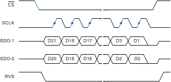 Figure 70. SPI-00-D-EDL Protocol
 Figure 72. SPI-00-Q-EDL Protocol
 Figure 71. SPI-10-D-EDL Protocol
 Figure 73. SPI-10-Q-EDL Protocol
When using any of the SPI-compatible protocols, the RVS output remains low throughout the data transfer frame; see the Timing Requirements and Switching Characteristics tables for associated timing parameters.
Figure 62 to Figure 73 illustrate how the wider data bus allows the host controller to read all 22 bits of the output data word using shorter data transfer frames. Table 7 and Table 8 show the number of SCLK required in an optimal read frame for the different output protocol selections.
NOTE
With SDO_CNTL[7:0] ≠ 00h or 01h, a long data transfer frame does not result in daisy-chain operation. On SDO pin (or pins), the 22 bits of output data word are followed by zeros.
7.5.4.2.3 Source-Synchronous (SRC) Protocols
As described in the Data Transfer Protocols section, the multiSPI digital interface supports an ADC-Clock-Master or a source-synchronous mode of data transfer between the device and host controller. In this mode, the device provides an output clock that is synchronous with the output data. Furthermore, the host controller can also select the output clock source, data bus width, and data transfer rate.
7.5.4.2.3.1 Output Clock Source Options with SRC Protocols
In all SRC protocols, the RVS pin provides the output clock. The device allows this output clock to be synchronous to either the external clock provided on the SCLK pin or to the internal clock of the device. Furthermore, this internal clock can be divided by a factor of two or four to lower the data rates.
As shown in Figure 74, set the SSYNC_CLK_SEL[1:0] bits in the SDO_CNTL register to select the output clock source.
 Figure 74. Output Clock Source Options With SRC Protocols
7.5.4.2.3.2 Bus Width Options With SRC Protocols
The device provides an option to increase the SDO bus width from one bit (default, single SDO) to two bits (dual SDO) or to four bits (quad SDO) when operating with any of the SRC protocols. Set the SDO_WIDTH[1:0] bits in the SDO_CNTL register to select the SDO bus width.
In dual-SDO mode (SDO_WIDTH[1:0] = 10b), two bits of data are launched on the two SDO pins (SDO-0 and SDO-1) on every SCLK rising edge.
In quad-SDO mode (SDO_WIDTH[1:0] = 11b), four bits of data are launched on the four SDO pins (SDO-0, SDO-1, SDO-2, and SDO-3) on every SCLK rising edge.
7.5.4.2.3.3 Output Data Rate Options With SRC Protocols
The device provides an option to transfer the data to the host controller at a single data rate (default, SDR) or at a double data rate (DDR). Set the DATA_RATE bit in the SDO_CNTL register to select the data transfer rate.
In SDR mode (DATA_RATE = 0b), the RVS pin toggles from low to high, and the output data bits are launched on the SDO pins on the output clock rising edge.
In DDR mode (DTA_RATE = 1b), the RVS pin toggles (from low-to-high or high-to-low), and the output data bits are launched on the SDO pins on every output clock edge, starting with the first rising edge.
The device supports all 24 combinations of output clock source, bus width, and output data rate, as shown in Table 9.
Table 9. SRC Protocol Combinations
| PROTOCOL | OUTPUT CLOCK SOURCE | BUS WIDTH | OUTPUT DATA RATE | SDI_CNTL | SDO_CNTL | #OUTPUT CLOCK (Optimal Read Frame) |
TIMING DIAGRAM |
|---|---|---|---|---|---|---|---|
| SRC-EXT-SS | SCLK(3) | Single | SDR | 00h, 01h, 02h, or 03h(1) |
03h | 10 | Figure 75 |
| SRC-INT-SS | INTCLK(2) | Single | SDR | 43h | 10 | Figure 76 | |
| SRC-IB2-SS | INTCLK / 2(2) | Single | SDR | 83h | 10 | ||
| SRC-IB4-SS | INTCLK / 4(2) | Single | SDR | C3h | 10 | ||
| SRC-EXT-DS | SCLK(3) | Dual | SDR | 0Bh | 10 | Figure 79 | |
| SRC-INT-DS | INTCLK(2) | Dual | SDR | 4Bh | 10 | Figure 80 | |
| SRC-IB2-DS | INTCLK / 2(2) | Dual | SDR | 8Bh | 10 | ||
| SRC-IB4-DS | INTCLK / 4(2) | Dual | SDR | CBh | 10 | ||
| SRC-EXT-QS | SCLK(3) | Quad | SDR | 0Fh | 5 | Figure 83 | |
| SRC-INT-QS | INTCLK(2) | Quad | SDR | 4Fh | 5 | Figure 84 | |
| SRC-IB2-QS | INTCLK / 2(2) | Quad | SDR | 8Fh | 5 | ||
| SRC-IB4-QS | INTCLK / 4(2) | Quad | SDR | CFh | 5 | ||
| SRC-EXT-SD | SCLK(3) | Single | DDR | 13h | 10 | Figure 77 | |
| SRC-INT-SD | INTCLK(2) | Single | DDR | 53h | 10 | Figure 78 | |
| SRC-IB2-SD | INTCLK / 2(2) | Single | DDR | 93h | 10 | ||
| SRC-IB4-SD | INTCLK / 4(2) | Single | DDR | D3h | 10 | ||
| SRC-EXT-DD | SCLK(3) | Dual | DDR | 1Bh | 5 | Figure 81 | |
| SRC-INT-DD | INTCLK(2) | Dual | DDR | 5Bh | 5 | Figure 82 | |
| SRC-IB2-DD | INTCLK / 2(2) | Dual | DDR | 9Bh | 5 | ||
| SRC-IB4-DD | INTCLK / 4(2) | Dual | DDR | DBh | 5 | ||
| SRC-EXT-QD | SCLK(3) | Quad | DDR | 1Fh | 3 | Figure 85 | |
| SRC-INT-QD | INTCLK(2) | Quad | DDR | 5Fh | 3 | Figure 86 | |
| SRC-IB2-QD | INTCLK / 2(2) | Quad | DDR | 9Fh | 3 | ||
| SRC-IB4-QD | INTCLK / 4(2) | Quad | DDR | DFh | 3 |
Figure 75 to Figure 86 show the details of various source synchronous protocols. Table 9 shows the number of output clocks required in an optimal read frame for the different output protocol selections.
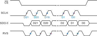 Figure 75. SRC-EXT-SS: SRC, SCLK, Single SDO, SDR
 Figure 77. SRC-EXT-SD: SRC, SCLK, Single SDO, DDR
 Figure 79. SRC-EXT-DS: SRC, SCLK, Dual SDO, SDR
 Figure 76. SRC-INT-SS: SRC, INTCLK, Single SDO, SDR
 Figure 78. SRC-INT-SD: SRC, INTCLK, Single SDO, DDR
 Figure 80. SRC-INT-DS: SRC, INTCLK, Dual SDO, SDR
 Figure 81. SRC-EXT-DD: SRC, SCLK, Dual SDO, DDR
 Figure 83. SRC-EXT-QS: SRC, SCLK, Quad SDO, SDR
 Figure 85. SRC-EXT-QD: SRC, SCLK, Quad SDO, DDR
 Figure 82. SRC-INT-DD: SRC, INTCLK, Dual SDO, DDR
 Figure 84. SRC-INT-QS: SRC, INTCLK, Quad SDO, SDR
 Figure 86. SRC-INT-QD: SRC, INTCLK, Quad SDO, DDR
7.5.5 Device Setup
The multiSPI digital interface and the device configuration registers offer multiple operation modes. This section describes how to select the hardware connection topology to meet different system requirements.
7.5.5.1 Single Device: All multiSPI Options
Figure 87 shows the connections between a host controller and a single device in order to exercise all options provided by the multiSPI digital interface.
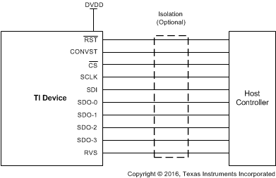 Figure 87. MultiSPI Digital Interface, All Pins
7.5.5.2 Single Device: Minimum Pins for a Standard SPI Interface
Figure 88 shows the minimum-pin interface for applications using a standard SPI protocol.
 Figure 88. SPI Interface, Minimum Pins
The CS, SCLK, SDI, and SDO-0 pins constitute a standard SPI port of the host controller. The CONVST pin is tied to CS, and the RST pin is tied to DVDD. The SDO-1, SDO-2, and SDO-3 pins have no external connections. The following features are also available:
- Control the CONVST pin independently to get additional timing flexibility.
- Control RST pin independently to add asynchronous reset functionality.
- Monitor the RVS pin for additional timing benefits.
7.5.5.3 Multiple Devices: Daisy-Chain Topology
A typical connection diagram showing multiple devices in a daisy-chain topology is shown in Figure 89.
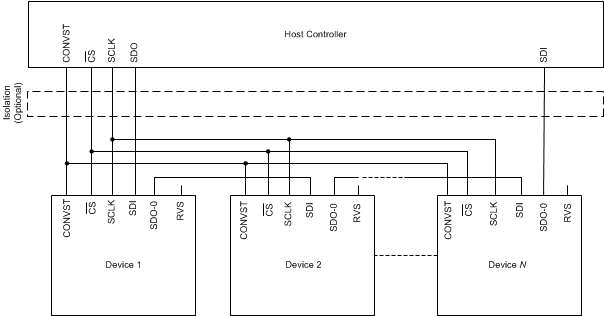 Figure 89. Daisy-Chain Connections
The CONVST, CS, and SCLK inputs of all devices are connected together and controlled by a single CONVST, CS, and SCLK pin of the host controller, respectively. The SDI input pin of the first device in the chain (Device 1) is connected to the SDO pin of the host controller, the SDO-0 output pin of Device 1 is connected to the SDI input pin of Device 2, and so on. The SDO-0 output pin of the last device in the chain (Device N) is connected to the SDI pin of the host controller.
To operate multiple devices in a daisy-chain topology, the host controller sets the configuration registers in each device with identical values and operates with any of the legacy, SPI-compatible protocols for data-read and data-write operations (SDO_CNT[7:0] = 00h or 01h). With these configurations settings, the 22-bit ODR and 22-bit IDR registers in each device collapse to form a single, 22-bit unified shift register (USR) per device, as shown in Figure 90.
 Figure 90. Unified Shift Register
All devices in the daisy-chain topology sample the respective device analog input signals on the CONVST rising edge. The data transfer frame starts with a CS falling edge. On each SCLK launch edge, every device in the chain shifts out the MSB of the respective USR on to the respective SDO-0 pin. On every SCLK capture edge, each device in the chain shifts in data received on the respective SDI pin as the LSB bit of the respective USR. Therefore, in a daisy-chain configuration, the host controller receives the data of Device N, followed by the data of Device N – 1, and so on (MSB-first). On the CS rising edge, each device decodes the contents in the respective USR, and takes appropriate action.
A typical timing diagram for three devices connected in daisy-chain topology using the SPI-00-S protocol is shown in Figure 91.
 Figure 91. Three-Device, Daisy-Chain Timing
In daisy-chain topology, the overall throughput of the system is proportionally reduced as more devices are connected in the daisy-chain.
NOTE
For N devices connected in daisy-chain topology, an optimal data transfer frame must contain 22 × N SCLK capture edges. For a longer data transfer frame (number of SCLK in the frame > 22 × N), the host controller must appropriately align the configuration data for each device before bringing CS high. A shorter data transfer frame (number of SCLK in the frame < 22 × N) might result in an erroneous device configuration, and must be avoided.
7.5.5.4 Multiple Devices: Star Topology
A typical connection diagram showing multiple devices in a star topology is shown in Figure 92. The CONVST, SDI, and SCLK inputs of all devices are connected together, and are controlled by a single CONVST, SDO, and SCLK pin of the host controller, respectively. Similarly, the SDO output pin of all devices are tied together and connected to the a single SDI input pin of the host controller. The CS input pin of each device is individually controlled by separate CS control lines from the host controller.
 Figure 92. Star-Topology Connection
The timing diagram for three devices connected in the star topology is shown in Figure 93. In order to avoid any conflict related to multiple devices driving the SDO line at the same time, make sure that the host controller pulls down the CS signal for only one device at any particular time.
 Figure 93. Three-Device, Star Connection Timing
7.6 Register Maps
7.6.1 Device Configuration and Register Maps
The device features nine configuration registers, mapped as described in Table 10.
Table 10. Configuration Registers Mapping
| ADDRESS | REGISTER NAME | REGISTER DESCRIPTION |
|---|---|---|
| 004h | PD_CNTL | Low-power modes control |
| 008h | SDI_CNTL | SDI input protocol selection |
| 00Ch | SDO_CNTL | SDO output protocol selection |
| 010h | DATA_CNTL | Output data word configuration |
| 014h | PATN_LSB | Eight least significant bits (LSB) of the output pattern |
| 015h | PATN_MID | Eight middle bits of the output pattern |
| 016h | PATN_MSB | Four most significant bits (MSB) of the output pattern |
| 020h | OFST_CAL | Offset calibration |
| 030h | REF_MRG | Reference margin |
7.6.1.1 PD_CNTL Register (address = 04h) [reset = 00h]
This register controls the low-power modes offered by the device.
| 7 | 6 | 5 | 4 | 3 | 2 | 1 | 0 |
| 0 | 0 | 0 | 0 | 0 | PD_REFBUF | PD_ADC | 0 |
| R-0b | R-0b | R-0b | R-0b | R-0b | R/W-0b | R/W-0b | R-0b |
| LEGEND: R/W = Read/Write; R = Read only; -n = value after reset |
Table 11. PD_CNTL Register Field Descriptions
| Bit | Field | Type | Reset | Description |
|---|---|---|---|---|
| 7-3 | 0 | R | 00000b | Reserved bits. Reads return 00000b. |
| 2 | PD_REFBUF | R/W | 0b | This bit powers down the internal reference buffer. 0b = Internal reference buffer is powered up 1b = Internal reference buffer is powered down |
| 1 | PD_ADC | R/W | 0b | This bit powers down the converter module. 0b = converter module is powered up 1b = converter module is powered down |
| 0 | 0 | R | 0b | Reserved bits. Do not write. Reads return 0b. |
To power-down the converter module, set the PD_ADC bit in the PD_CNTL register. The converter module powers down on the rising edge of CS. To power-up the converter module, reset the PD_ADC bit in the PD_CNTL register. The converter module starts to power-up on the rising edge of CS. Wait for tPU_ADC before initiating any conversion or data transfer operation.
To power-down the internal reference buffer, set the PD_REFBUF bit in the PD_CNTL register. The internal reference buffer powers down on the rising edge of CS. To power-up the internal reference buffer, reset the PD_REFBUF bit in the PD_CNTL register. The internal reference buffer starts to power-up on the rising edge of CS. Wait for tPU_REFBUF before initiating any conversion.
7.6.1.2 SDI_CNTL Register (address = 008h) [reset = 00h]
This register selects the SPI protocol for writing data to the device.
| 7 | 6 | 5 | 4 | 3 | 2 | 1 | 0 |
| 0 | 0 | 0 | 0 | 0 | 0 | SDI_MODE[1:0] | |
| R-0b | R-0b | R-0b | R-0b | R-0b | R-0b | R/W-00b | |
| LEGEND: R/W = Read/Write; R = Read only; -n = value after reset |
Table 12. SDI_CNTL Register Field Descriptions
| Bit | Field | Type | Reset | Description |
|---|---|---|---|---|
| 7-2 | 0 | R | 000000b | Reserved bits. Do not write. Reads return 000000b. |
| 1-0 | SDI_MODE[1:0] | R/W | 00b | These bits select the protocol for writing data into the device. 00b = Standard SPI with CPOL = 0 and CPHASE = 0 01b = Standard SPI with CPOL = 0 and CPHASE = 1 10b = Standard SPI with CPOL = 1 and CPHASE = 0 11b = Standard SPI with CPOL = 1 and CPHASE = 1 |
7.6.1.3 SDO_CNTL Register (address = 0Ch) [reset = 00h]
This register configures the protocol for reading data from the device.
| 7 | 6 | 5 | 4 | 3 | 2 | 1 | 0 |
| SSYNC_CLK_SEL[1:0] | 0 | DATA_RATE | SDO_WIDTH[1:0] | SDO_MODE[1:0] | |||
| R/W-00b | R-0b | R/W-0b | R/W-00b | R/W-00b | |||
| LEGEND: R/W = Read/Write; R = Read only; -n = value after reset |
Table 13. SDO_CNTL Register Field Descriptions
| Bit | Field | Type | Reset | Description |
|---|---|---|---|---|
| 7-6 | SSYNC_CLK_SEL[1:0] | R/W | 00b | These bits select the source and frequency of the clock for the ADC-Clock-Master mode, and are valid only if SDO_MODE[1:0] = 11b. 00b = External SCLK echo 01b = Internal clock (INTCLK) 10b = Internal clock / 2 (INTCLK / 2) 11b = Internal clock / 4 (INTCLK / 4) |
| 5 | 0 | R | 0b | Reserved bit. Do not write. Reads return 0b. |
| 4 | DATA_RATE | R/W | 0b | This bit is ignored if SDO_MODE[1:0] = 00b. When SDO_MODE[1:0] = 11b: 0b = SDOs are updated at single data rate (SDR) with respect to the output clock 1b = SDOs are updated at double data rate (DDR) with respect to the output clock |
| 3-2 | SDO_WIDTH[1:0] | R/W | 00b | These bits set the width of the output bus. 0xb = Data are output only on SDO-0 10b = Data are output only on SDO-0 and SDO-1 11b = Data are output on SDO-0, SDO-1, SDO-2, and SDO-3 |
| 1-0 | SDO_MODE[1:0] | R/W | 00b | These bits select the protocol for reading data from the device. 00b = SDO follows the SPI protocol selected in the SDI_CNTL register 01b = SDO follows the SPI protocol selected in the SDI_CNTL register but with Early Data Launch feature enabled. See Table 6. 10b = Invalid configuration, not supported by the device 11b = SDO follows the source-synchronous protocol |
7.6.1.4 DATA_CNTL Register (address = 010h) [reset = 00h]
This register configures the contents of the 22-bit output data word (D[21:0]).
| 7 | 6 | 5 | 4 | 3 | 2 | 1 | 0 |
| 0 | 0 | 0 | 0 | FPAR_LOC[1:0] | PAR_EN | DATA_VAL | |
| R-0b | R-0b | R-0b | R-0b | R/W-00b | R/W-0b | R/W-0b | |
| LEGEND: R/W = Read/Write; R = Read only; -n = value after reset |
Table 14. DATA_CNTL Register Field Descriptions
| Bit | Field | Type | Reset | Description |
|---|---|---|---|---|
| 7-4 | 0 | R | 0000b | Reserved bits. Reads return 0000b. |
| 3-2 | FPAR_LOC[1:0] | R/W | 00b | These bits control the data span for calculating the FTPAR bit (bit D[0] in the output data word). 00b = D[0] reflects even parity calculated for 4 MSB 01b = D[0] reflects even parity calculated for 8 MSB 10b = D[0] reflects even parity calculated for 12 MSB 11b = D[0] reflects even parity calculated for 16 MSB |
| 1 | PAR_EN | R/W | 0b | 0b = Output data does not contain any parity information D[1] = 0 D[0] = 0 1b = Parity information is appended to the LSB of the output data D[1] = Even parity calculated on bits D[21:2] D[0] = Even parity computed on selected number of MSB of D[21:2] as per FPAR_LOC[1:0] setting See Figure 44 for further details of parity computation. |
| 0 | DATA_VAL | R/W | 0b | These bits control bits D[21:2] of the output data word. 0b = 20-bit conversion output 1b = 20-bit contents of the fixed-pattern registers See PATN CNTL for more details. |
7.6.1.5 PATN_LSB Register (address = 014h) [reset = 00h]
This register controls the eight LSB of the output pattern when DATA_VAL = 1b; see Figure 101.
| 7 | 6 | 5 | 4 | 3 | 2 | 1 | 0 |
| PATN_LSB_BITS | |||||||
| R/W-00000000b | |||||||
| LEGEND: R/W = Read/Write; R = Read only; -n = value after reset |
Table 15. PATN_LSB Register Field Descriptions
| Bit | Field | Type | Reset | Description |
|---|---|---|---|---|
| 7-0 | PATN_LSB_BITS | R/W | 00000000b | 8 LSB of the output pattern |
7.6.1.6 PATN_MID Register (address = 015h) [reset = 00h]
This register controls the middle eight bits of the output pattern when DATA_VAL = 1b; see Figure 101.
| 7 | 6 | 5 | 4 | 3 | 2 | 1 | 0 |
| PATN_MID_BITS | |||||||
| R/W-00000000b | |||||||
| LEGEND: R/W = Read/Write; R = Read only; -n = value after reset |
Table 16. PATN_MID Register Field Descriptions
| Bit | Field | Type | Reset | Description |
|---|---|---|---|---|
| 7-0 | PATN_MID_BITS | R/W | 00000000b | 8 middle bits of the output pattern |
7.6.1.7 PATN_MSB Register (address = 016h) [reset = 00h]
This register controls the four MSB of the output pattern when DATA_VAL = 1b; see Figure 101.
| 7 | 6 | 5 | 4 | 3 | 2 | 1 | 0 |
| 0 | 0 | 0 | 0 | PATN_MSB_BITS | |||
| R-0b | R-0b | R-0b | R-0b | R/W-0000b | |||
| LEGEND: R/W = Read/Write; R = Read only; -n = value after reset |
Table 17. PATN_MSB Register Field Descriptions
| Bit | Field | Type | Reset | Description |
|---|---|---|---|---|
| 7-4 | 0 | R | 0000b | Reserved bits. Reads return 0000b. |
| 3-0 | PATN_MSB_BITS | R/W | 0000b | 4 MSB of the output pattern |
![ADS8900B ADS8902B ADS8904B DATA_PATN[19:0] ADS8900B ADS8902B ADS8904B data_patn_20_bas707.gif](/ods/images/JAJSCN8A/data_patn_20_bas707.gif) Figure 101. DATA_PATN[19:0]
Figure 101. DATA_PATN[19:0]
7.6.1.8 OFST_CAL Register (address = 020h) [reset = 00h]
This register selects the external reference range for optimal offset calibration.
| 7 | 6 | 5 | 4 | 3 | 2 | 1 | 0 |
| 0 | 0 | 0 | 0 | 0 | REF_SEL[2:0] | ||
| R-0b | R-0b | R-0b | R-0b | R-0b | R/W-000b | ||
| LEGEND: R/W = Read/Write; R = Read only; -n = value after reset |
Table 18. OFST_CAL Register Field Descriptions
| Bit | Field | Type | Reset | Description |
|---|---|---|---|---|
| 7-3 | 0 | R | 00000b | Reserved bits. Reads return 00000b. |
| 2-0 | REF_SEL[2:0] | R/W | 000b | These bits select the external reference range for optimal offset. 000b = Optimum offset calibration for VREF = 5.0 V 001b = Optimum offset calibration for VREF = 4.5 V 010b = Optimum offset calibration for VREF = 4.096 V 011b = Optimum offset calibration for VREF = 3.3 V 100b = Optimum offset calibration for VREF = 3.0 V 101b = Optimum offset calibration for VREF = 2.5 V 110b = Optimum offset calibration for VREF = 5.0 V 111b = Optimum offset calibration for VREF = 5.0 V |
7.6.1.9 REF_MRG Register (address = 030h) [reset = 00h]
This register selects the margining to be added to or subtracted from the reference buffer output; see the Reference Buffer Module section.
| 7 | 6 | 5 | 4 | 3 | 2 | 1 | 0 |
| 0 | 0 | EN_MARG | REF_OFST[4:0] | ||||
| R-0b | R-0b | R/W-0b | R/W-00000b | ||||
| LEGEND: R/W = Read/Write; R = Read only; -n = value after reset |
Table 19. REF_MRG Register Field Descriptions
| Bit | Field | Type | Reset | Description |
|---|---|---|---|---|
| 7-6 | 0 | R | 00b | Reserved bits. Reads return 00b. |
| 5 | EN_MARG | R/W | 0b | This bit enables margining feature. 0b = Margining is disabled 1b = Margining is enabled |
| 4-0 | REF_OFST[4:0] | R/W | 00000b | These bits select the reference offset value as per Table 20. |
Table 20. REF_OFST[4:0] settings
| REF_OFST[4:0] | ΔVREFBUFOUT (typical(1)) |
|---|---|
| 00000b | 0 mV |
| 00001b | 280 µV |
| 00010b | 580 µV |
| 00011b | 840 µV |
| 00100b | 1.12 mV |
| 00101b | 1.4 mV |
| 00110b | 1.68 mV |
| 00111b | 1.96 mV |
| 01000b | 2.24 mV |
| 01001b | 2.52 mV |
| 01010b | 2.8 mV |
| 01011b | 3.08 mV |
| 01100b | 3.36 mV |
| 01101b | 3.64 mV |
| 01110b | 3.92 mV |
| 01111b | 4.2 mV |
| 10000b | –4.5 mV |
| 10001b | –4.22 mV |
| 10010b | –3.94 mV |
| 10011b | –3.66 mV |
| 10100b | –3.38 mV |
| 10101b | –3.1 mV |
| 10110b | –2.82 mV |
| 10111b | –2.54 mV |
| 11000b | –2.26 mV |
| 11001b | –1.98 mV |
| 11010b | –1.7 mV |
| 11011b | –1.42 mV |
| 11100b | –1.14 mV |
| 11101b | –860 µV |
| 11110b | –580 µV |
| 11111b | –280 µV |