JAJSCN8A November 2016 – June 2017 ADS8900B , ADS8902B , ADS8904B
PRODUCTION DATA.
- 1 特長
- 2 アプリケーション
- 3 概要
- 4 改訂履歴
- 5 Pin Configuration and Functions
- 6 Specifications
-
7 Detailed Description
- 7.1 Overview
- 7.2 Functional Block Diagram
- 7.3 Feature Description
- 7.4 Device Functional Modes
- 7.5
Programming
- 7.5.1 Output Data Word
- 7.5.2 Data Transfer Frame
- 7.5.3 Interleaving Conversion Cycles and Data Transfer Frames
- 7.5.4 Data Transfer Protocols
- 7.5.5 Device Setup
- 7.6
Register Maps
- 7.6.1
Device Configuration and Register Maps
- 7.6.1.1 PD_CNTL Register (address = 04h) [reset = 00h]
- 7.6.1.2 SDI_CNTL Register (address = 008h) [reset = 00h]
- 7.6.1.3 SDO_CNTL Register (address = 0Ch) [reset = 00h]
- 7.6.1.4 DATA_CNTL Register (address = 010h) [reset = 00h]
- 7.6.1.5 PATN_LSB Register (address = 014h) [reset = 00h]
- 7.6.1.6 PATN_MID Register (address = 015h) [reset = 00h]
- 7.6.1.7 PATN_MSB Register (address = 016h) [reset = 00h]
- 7.6.1.8 OFST_CAL Register (address = 020h) [reset = 00h]
- 7.6.1.9 REF_MRG Register (address = 030h) [reset = 00h]
- 7.6.1
Device Configuration and Register Maps
-
8 Application and Implementation
- 8.1 Application Information
- 8.2 Typical Application
- 9 Power-Supply Recommendations
- 10Layout
- 11デバイスおよびドキュメントのサポート
- 12メカニカル、パッケージ、および注文情報
パッケージ・オプション
メカニカル・データ(パッケージ|ピン)
- RGE|24
サーマルパッド・メカニカル・データ
- RGE|24
発注情報
6 Specifications
6.1 Absolute Maximum Ratings
over operating free-air temperature range (unless otherwise noted)(1)| MIN | MAX | UNIT | |
|---|---|---|---|
| RVDD to GND | –0.3 | 7 | V |
| DVDD to GND | –0.3 | 7 | V |
| REFIN to REFM | –0.3 | RVDD + 0.3 | V |
| REFM to GND | –0.1 | 0.1 | V |
| Analog Input (AINP, AINM) to GND | –0.3 | VREF + 0.3 | V |
| Digital input (RST, CONVST, CS, SCLK, SDI) to GND | –0.3 | DVDD + 0.3 | V |
| Digital output (READY, SDO-0, SDO-1, SDO-2, SDO-3) to GND | –0.3 | DVDD + 0.3 | V |
| Analog Input (AINP, AINM) to RVDD and GND | –130 | 130 | mA |
| Operating free-air temperature, TA | –40 | 125 | °C |
| Storage temperature, Tstg | –65 | 150 | °C |
(1) Stresses beyond those listed under Absolute Maximum Ratings may cause permanent damage to the device. These are stress ratings only, which do not imply functional operation of the device at these or any other conditions beyond those indicated under Recommended Operating Conditions. Exposure to absolute-maximum-rated conditions for extended periods may affect device reliability.
6.2 ESD Ratings
| VALUE | UNIT | |||
|---|---|---|---|---|
| V(ESD) | Electrostatic discharge | Human-body model (HBM), per ANSI/ESDA/JEDEC JS-001(1) | ±2000 | V |
| Charged-device model (CDM), per JEDEC specification JESD22-C101(2) | ±500 | |||
(1) JEDEC document JEP155 states that 500-V HBM allows safe manufacturing with a standard ESD control process.
(2) JEDEC document JEP157 states that 250-V CDM allows safe manufacturing with a standard ESD control process.
6.3 Recommended Operating Conditions
over operating free-air temperature range (unless otherwise noted)6.4 Thermal Information
| THERMAL METRIC(1) | ADS890xB | UNITS | |
|---|---|---|---|
| RGE (VQFN) | |||
| 24 PINS | |||
| RθJA | Junction-to-ambient thermal resistance | 31.9 | °C/W |
| RθJC(top) | Junction-to-case (top) thermal resistance | 29.9 | °C/W |
| RθJB | Junction-to-board thermal resistance | 8.9 | °C/W |
| ψJT | Junction-to-top characterization parameter | 0.3 | °C/W |
| ψJB | Junction-to-board characterization parameter | 8.9 | °C/W |
| RθJC(bot) | Junction-to-case (bottom) thermal resistance | 2.0 | °C/W |
(1) For more information about traditional and new thermal metrics, see the Semiconductor and IC Package Thermal Metrics application report.
6.5 Electrical Characteristics
At RVDD = 5.5 V, DVDD = 1.65 V to 5.5 V, VREF = 5 V, and maximum throughput (unless otherwise noted).Minimum and maximum values at TA = –40°C to +125°C; typical values at TA = 25°C.
| PARAMETER | TEST CONDITIONS | MIN | TYP | MAX | UNIT | |
|---|---|---|---|---|---|---|
| ANALOG INPUT | ||||||
| FSR | Full-scale input range (AINP – AINM) |
–VREF | VREF | V | ||
| VIN | Absolute input voltage (AINP and AINM to REFM) |
0 | VREF | V | ||
| VCM | Common-mode voltage (AINP + AINM) / 2 |
(VREF / 2) – 0.1 | VREF / 2 | (VREF / 2) + 0.1 | V | |
| CIN | Input capacitance | Sample mode | 60 | pF | ||
| Hold mode | 4 | pF | ||||
| VOLTAGE REFERENCE INPUT (REFIN) | ||||||
| IREF | Reference input current | VREF = 5 V | 0.1 | 1 | µA | |
| CREF | Internal capacitance | 10 | pF | |||
| REFERENCE BUFFER OUTPUT (REFBUFOUT) | ||||||
| V(RO) | Reference buffer offset voltage (VREFBUFOUT – VREF) |
With EN_MARG = 0b(1), TA = 25°C(5) | –250 | 250 | µV | |
| CREFBUF | External ceramic decoupling capacitor | 10 | 22 | µF | ||
| RESR | External series resistor | 0 | 1 | 1.3 | Ω | |
| ISHRT | Short-circuit current | 30 | mA | |||
| Margining range | With EN_MARG = 1b(1) | ±4.5 | mV | |||
| Margining resolution | With EN_MARG = 1b(1) | 280 | µV | |||
| DC ACCURACY(2) (CREFBUF = 22 µF, RESR = 1 Ω) | ||||||
| Resolution | 20 | Bits | ||||
| NMC | No missing codes | 20 | Bits | |||
| INL | Integral nonlinearity(3) | TA = 0°C to +60°C | -2 | ±1 | 2 | ppm(4) |
| TA = –40°C to +85°C | -2.75 | ±1 | 2.75 | |||
| TA = –40°C to +125°C | -3.75 | ±1 | 3.75 | |||
| DNL | Differential nonlinearity(3) | -0.5 | ±0.2 | 0.5 | ppm(4) | |
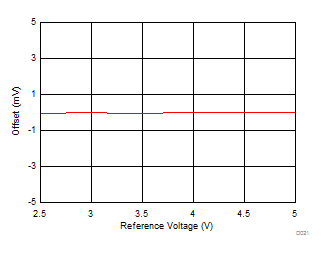
| E(IO) | Input offset error(3) | TA = 25°C(5) | -11.5 | ±3 | 11.5 | ppm(4) |
| TA = –40°C to +125°C(5) | -60 | ±10 | 60 | |||
| dVOS/dT | Input offset thermal drift(5) | 1 | μV/°C | |||
| GE | Gain error(3) | EN_MARG = 0b(1)(6) | -0.03 | ±0.005 | 0.03 | %FSR |
| dGE/dT | Gain error thermal drift | EN_MARG = 0b(1)(6) | 3.6 | ppm/°C | ||
| TNS | Transition noise | 2.3 | ppm(4) | |||
| First output code deviation for burst-mode data acquisition |
See Reference Buffer Module | –3 | 3 | TNS | ||
| CMRR | Common-mode rejection ratio | dc to 20 kHz | 80 | dB | ||
| SAMPLING DYNAMICS | ||||||
| Aperture delay | 4 | ns | ||||
| tj-rms | Aperture jitter | 2 | ps RMS | |||
| f3-DB(small) | Small-signal bandwidth | 23 | MHz | |||
| AC ACCURACY(2)(7) (CREFBUF = 22 µF, RESR = 1 Ω) | ||||||
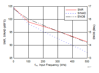
| SINAD | Signal-to-noise + distortion | fIN = 2 kHz, TA = –40°C to +85°C | 101.8 | 103.9 | dB | |
| fIN = 2 kHz, TA = –40°C to +125°C | 101.3 | 103.9 | ||||
| SNR | Signal-to-noise ratio | fIN = 2 kHz, TA = –40°C to +85°C | 102 | 104.5 | dB | |
| fIN = 2 kHz, TA = –40°C to +125°C | 101.5 | 104.5 | ||||
| fIN = 100 kHz | 99.5 | |||||
| THD | Total harmonic distortion | fIN = 2 kHz | –125 | dB | ||
| fIN = 100 kHz | –110 | |||||
| SFDR | Spurious-free dynamic range | fIN = 2 kHz | 125 | dB | ||
| LDO OUTPUT (DECAP) | ||||||
| VLDO | LDO output voltage (DECAP pins) |
2.85 | V | |||
| CLDO | External ceramic capacitor on DECAP pins | 1 | µF | |||
| tPU_LDO | LDO power-up time | CLDO = 1 µF, RVDD > VLDO | 1 | ms | ||
| ISHRT-LDO | Short-circuit current | 100 | mA | |||
| DIGITAL INPUTS | ||||||
| VIH | High-level input voltage | 1.65 V < DVDD < 2.3 V | 0.8 DVDD | DVDD + 0.3 | V | |
| 2.3 V < DVDD < 5.5 V | 0.7 DVDD | DVDD + 0.3 | ||||
| VIL | Low-level input voltage | 1.65 V < DVDD < 2.3 V | –0.3 | 0.2 DVDD | V | |
| 2.3 V < DVDD < 5.5 V | –0.3 | 0.3 DVDD | ||||
| Input current | ±0.01 | 0.1 | μA | |||
| DIGITAL OUTPUTS | ||||||
| VOH | High-level output voltage | IOH = 500-µA source | 0.8 DVDD | DVDD | V | |
| VOL | Low-level output voltage | IOH = 500-µA sink | 0 | 0.2 DVDD | V | |
| POWER SUPPLY | ||||||
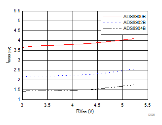
| IRVDD | Analog supply current | ADS8900B at RVDD = 5 V, 1-MSPS | 4.2 | 5.8 | mA | |
| ADS8902B at RVDD = 5 V, 500-KSPS | 3.2 | 4 | mA | |||
| ADS8904B at RVDD = 5 V, 250-KSPS | 2.8 | 3.6 | mA | |||
| Static, no conversion | 970 | μA | ||||
| Static, PD_ADC = 1b(8) | 900 | μA | ||||
| Static, PD_REFBUF = 1b(8) | 120 | μA | ||||
| Static, PD_ADC = 1b and PD_REFBUF = 1b(8) | 40 | μA | ||||
| IDVDD | Digital supply current | DVDD = 3 V, CLOAD = 10 pF, no conversion | 1 | μA | ||
| PRVDD | Power dissipation | ADS8900B at RVDD = 5 V, 1-MSPS | 21 | 29 | mW | |
| ADS8902B at RVDD = 5 V, 500-KSPS | 16 | 20 | ||||
| ADS8904B at RVDD = 5 V, 250-KSPS | 14 | 18 | ||||
(1) See the REF_MRG Register.
(2) While operating with internal reference buffer and LDO.
(3) See for statistical distribution data for DNL, INL, offset, and gain error parameters.
(4) LSB = least-significant bit. 1 LSB at 20-bit resolution is approximately 0.95 ppm.
(5) For selected VREF, see the OFST_CAL Register.
(6) Includes internal reference buffer errors and drifts.
(7) For VIN = –0.1 dBFS.
(8) See the PD_CNTL Register.
6.6 Timing Requirements
| MIN | TYP | MAX | UNIT | TIMING DIAGRAM | |||
|---|---|---|---|---|---|---|---|
| CONVERSION CYCLE | |||||||
| fcycle | Sampling frequency | ADS8900B | 1000 | kHz | Figure 1 | ||
| ADS8902B | 500 | ||||||
| ADS8904B | 250 | ||||||
| tcycle | ADC cycle-time period | ADS8900B | 1 | µs | |||
| ADS8902B | 2 | ||||||
| ADS8904B | 4 | ||||||
| twh_CONVST | Pulse duration: CONVST high | 30 | ns | ||||
| twl_CONVST | Pulse duration: CONVST low | 30 | ns | ||||
| tacq | Acquisition time | 300 | ns | ||||
| tqt_acq | Quiet acquisition time | 30 | ns | Figure 46, see Data Transfer Protocols | |||
| td_cnvcap | Quiet aperture time | 20 | ns | ||||
| ASYNCHRONOUS RESET, AND LOW POWER MODES | |||||||
| twl_RST | Pulse duration: RST low | 100 | ns | Figure 2 | |||
| SPI-COMPATIBLE SERIAL INTERFACE | |||||||
| fCLK | Serial clock frequency | 2.35 V ≤ DVDD ≤ 5.5 V, TA = –40°C to +125°C, VIH > 0.7 DVDD, VIL < 0.3 DVDD |
70 | MHz | Figure 3 | ||
| 1.65 V ≤ DVDD < 2.35 V, TA = –40°C to +125°C, VIH > 0.8 DVDD, VIL < 0.2 DVDD |
20 | ||||||
| 1.65 V ≤ DVDD < 2.35 V, TA = 0°C to +60°C, VIH > 0.8 DVDD, VIL < 0.2 DVDD |
57 | ||||||
| 1.65 V ≤ DVDD < 2.35 V, TA = –40°C to +125°C, VIH > 0.9 DVDD, VIL < 0.1 DVDD |
68 | ||||||
| tCLK | Serial clock time period | 1/fCLK | ns | Figure 3 | |||
| tph_CK | SCLK high time | 0.45 | 0.55 | tCLK | Figure 3 | ||
| tpl_CK | SCLK low time | 0.45 | 0.55 | tCLK | |||
| tsu_CSCK | Setup time: CS falling to the first SCLK capture edge | 12 | ns | ||||
| tsu_CKDI | Setup time: SDI data valid to the SCLK capture edge | 1.5 | ns | ||||
| tht_CKDI | Hold time: SCLK capture edge to (previous) data valid on SDI | 1 | ns | ||||
| tht_CKCS | Delay time: last SCLK falling to CS rising | 7 | ns | ||||
| SOURCE-SYNCHRONOUS SERIAL INTERFACE (External Clock)(1) | |||||||
| fCLK | Serial clock frequency | SDR (DATA_RATE = 0b), 2.35 V ≤ DVDD ≤ 5.5 V |
70 | MHz | Figure 4, see Data Transfer Protocols | ||
| DDR (DATA_RATE = 1b), 2.35 V ≤ DVDD ≤ 5.5 V |
35 | ||||||
| tCLK | Serial clock time period | 1/fCLK | ns | ||||
(1) The external clock option is not recommended when operating with DVDD < 2.35 V. See Table 9.
6.7 Switching Characteristics
At RVDD = 5.5 V, DVDD = 1.65 V to 5.5 V, VREF = 5 V, and maximum throughput (unless otherwise noted).Minimum and maximum values at TA = –40°C to +125°C; typical values at TA = 25°C.
| PARAMETER | MIN | TYP | MAX | UNIT | TIMING DIAGRAM | ||
|---|---|---|---|---|---|---|---|
| CONVERSION CYCLE | |||||||
| tconv | Conversion time | ADS8900B | 600 | 670 | ns | Figure 1 | |
| ADS8902B | 1100 | 1200 | |||||
| ADS8904B | 2400 | 2500 | |||||
| ASYNCHRONOUS RESET, AND LOW POWER MODES | |||||||
| td_rst | Delay time: RST rising to RVS rising | 3 | ms | Figure 2 | |||
| tPU_ADC | Power-up time for converter module | 1 | ms | See PD_CNTL Register | |||
| tPU_REFBUF | Power-up time for internal reference buffer, CREFBUF = 22 µF | 10 | ms | ||||
| tPU_Device | Power-up time for device | CLDO = 1 µF, CREFBUF = 22 µF | 10 | ms | |||
| SPI-COMPATIBLE SERIAL INTERFACE | |||||||
| tden_CSDO | Delay time: CS falling to data enable | 9 | ns | Figure 3 | |||
| tdz_CSDO | Delay time: CS rising to SDO going to Hi-Z | 10 | ns | ||||
| td_CKDO | Delay time: SCLK launch edge to (next) data valid on SDO | 13 | ns | ||||
| td_CSRDY_f | Delay time: CS falling to RVS falling | 12 | ns | Figure 4 | |||
| td_CSRDY_r | Delay time: CS rising to RVS rising |
After NOP operation | 30 | ns | Figure 4 | ||
| After WR or RD operation | 120 | ||||||
| SOURCE-SYNCHRONOUS SERIAL INTERFACE (External Clock)(1) | |||||||
| td_CKSTR_r | Delay time: SCLK launch edge to RVS rising | 13 | ns | Figure 4 | |||
| td_CKSTR_f | Delay time: SCLK launch edge to RVS falling | 13 | ns | ||||
| toff_STRDO_f | Time offset: RVS falling to (next) data valid on SDO | -2 | 2 | ns | |||
| toff_STRDO_r | Time offset: RVS rising to (next) data valid on SDO | -2 | 2 | ns | |||
| tph_STR | Strobe output high time, 2.35 V ≤ DVDD ≤ 5.5 V | 0.45 | 0.55 | tSTR | |||
| tpl_STR | Strobe output low time, 2.35 V ≤ DVDD ≤ 5.5 V | 0.45 | 0.55 | tSTR | |||
| SOURCE-SYNCHRONOUS SERIAL INTERFACE (Internal Clock) | |||||||
| td_CSSTR | Delay time: CS falling to RVS rising | 15 | 50 | ns | Figure 5 | ||
| tSTR | Strobe output time period | INTCLK option | 15 | ns | |||
| INTCLK / 2 option | 30 | ||||||
| INTCLK / 4 option | 60 | ||||||
| tph_STR | Strobe output high time | 0.45 | 0.55 | tSTR | |||
| tpl_STR | Strobe output low time | 0.45 | 0.55 | tSTR | |||
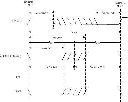 Figure 1. Conversion Cycle Timing
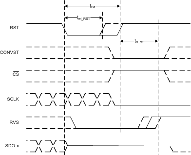 Figure 2. Asynchronous Reset Timing
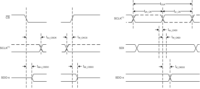
1. The SCLK polarity, launch edge, and capture edge depend on the SPI protocol selected.
Figure 3. SPI-Compatible Serial Interface Timing
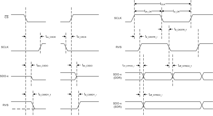 Figure 4. Source-Synchronous Serial Interface Timing (External Clock)
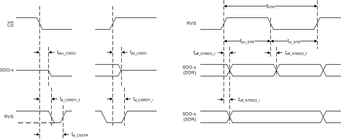 Figure 5. Source-Synchronous Serial Interface Timing (Internal Clock)
6.8 Typical Characteristics
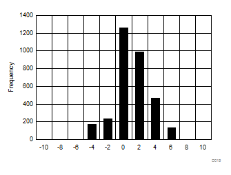
at TA = 25°C, RVDD = 5.5 V, DVDD = 3 V, VREF = 5 V, and maximum-rated throughput (unless otherwise noted)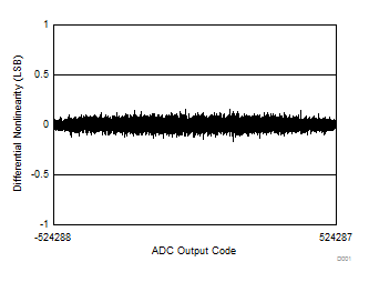
| Typical DNL = ±0.2 ppm |
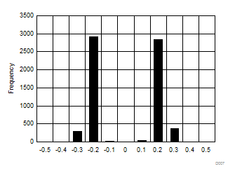
| 3250 devices |
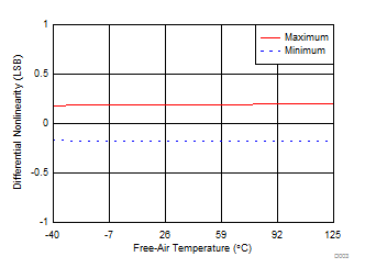
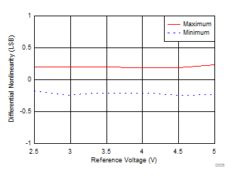
| 3250 devices |
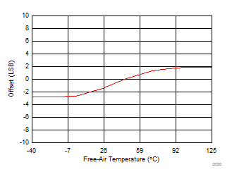
| REF_SEL[2:0] = 000b |
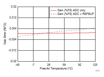
| EN_MARG = 0b |
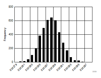
| Standard Deviation = 2 ppm |
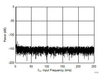
| fIN = 2 kHz | SNR = 104.5 dB | THD = –125 dB |
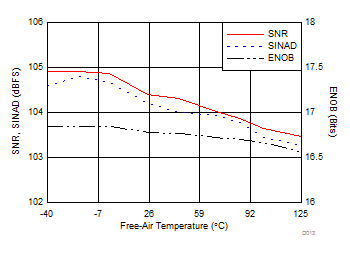
| fIN = 2 kHz |
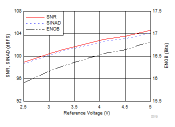
| fIN = 2 kHz |
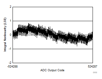
| Typical INL = ±0.75 ppm |
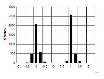
| 3250 devices |
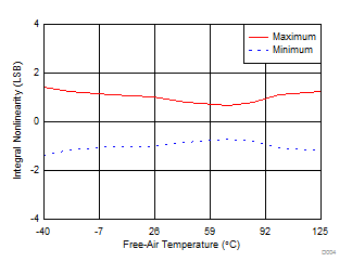
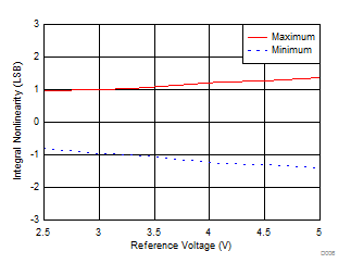
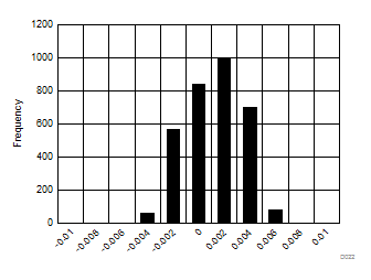
| 3250 devices |
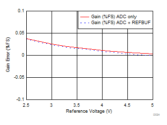
| EN_MARG = 0b |
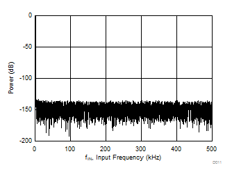
| fIN = 2 kHz | SNR = 104.5 dB | THD = –125 dB |
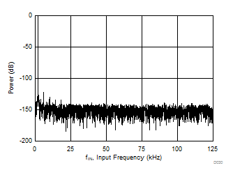
| fIN = 2 kHz | SNR = 104.5 dB | THD = –125 dB |
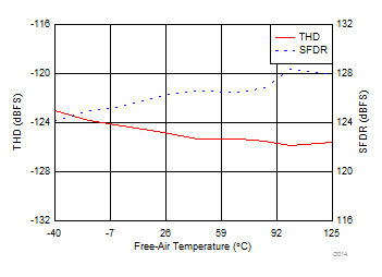
| fIN = 2 kHz |
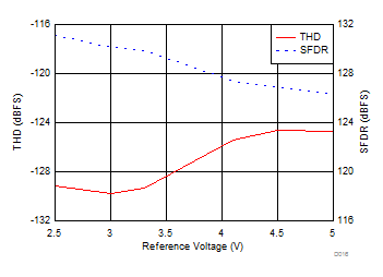
| fIN = 2 kHz |
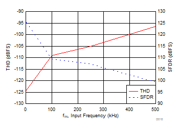
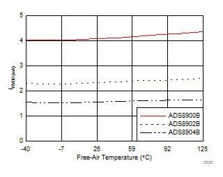
| RVDD = 5 V |
