JAJSVV8 December 2024 AFE5401-EP
PRODUCTION DATA
- 1
- 1 特長
- 2 アプリケーション
- 3 概要
- 4 Pin Configuration and Functions
-
5 Specifications
- 5.1 Absolute Maximum Ratings
- 5.2 ESD Ratings
- 5.3 Recommended Operating Conditions
- 5.4 Thermal Information
- 5.5 Electrical Characteristics
- 5.6 Digital Characteristics
- 5.7 Timing Requirements: Output Interface
- 5.8 Timing Requirements: RESET
- 5.9 Timing Requirements: Serial Interface Operation
- 5.10 Typical Characteristics
- 6 Parameter Measurement Information
-
7 Detailed Description
- 7.1 Overview
- 7.2 Functional Block Diagram
- 7.3 Feature Description
- 7.4 Device Functional Modes
- 7.5 Programming
- 7.6 Register Maps
- 8 Application and Implementation
- 9 Revision History
- 10Device and Documentation Support
- 11Mechanical, Packaging, and Orderable Information
7.3.8.2 Auxiliary Channel
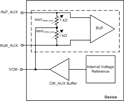
The auxiliary analog inputs (INIP_AUX, INIM _AUX) can be enabled instead of the INIP, INIM inputs using the AUX_CHI_EN bits (Table 7-9). The auxiliary analog input signal path consists of an input unity-gain buffer followed by an ADC. The LNA, PGA, equalizer, and antialiasing filter are bypassed and powered down in this mode. Figure 7-8 shows the internal block diagram for auxiliary channel mode. When this mode is enabled, the maximum input swing is limited to 2 VPP before the input becomes saturated or distorted.
| AUX_CHI_EN | DESCRIPTION |
|---|---|
| 0 | INIP, INIM active, analog |
| 1 | INIP _AUX, INIM_AUX |

The dc common-mode on the INIP_AUX, INIM _AUX pins are internally biased to the optimum voltage (referred to as VCM).
The dc common-mode biasing is set with two internal, programmable, single-ended resistors (RINTTERM_AUX). These resistors can be programmed to a higher value using the TERM_INT_20K_AUX register setting as described in Table 7-10.
| TERM_INT_20K_AUX | DESCRIPTION |
|---|---|
| 0 | RINTTERM_AUX = 1 kΩ |
| 1 | RINTTERM_AUX = 10 kΩ |
The auxiliary inputs can also be ac-coupled as a result of the internal common-mode setting. The external input ac-coupling capacitors form a high-pass filter with RINTTERM_AUX. Therefore, the capacitor values should allow the lowest frequency of interest to pass with minimum attenuation.
For typical frequencies greater than 1 MHz, a value of 50 nF or greater is recommended. For instances where the input signal cannot be ac-coupled because of system requirements, it is recommended to use the VCM output to set the dc common-mode of the input signal. The driving capability of VCM is limited. A 100-nF capacitor should be connected on each VCM input to AVSS.