SBASB81 December 2024 AFE5401-EP
PRODUCTION DATA
- 1
- 1 Features
- 2 Applications
- 3 Description
- 4 Pin Configuration and Functions
-
5 Specifications
- 5.1 Absolute Maximum Ratings
- 5.2 ESD Ratings
- 5.3 Recommended Operating Conditions
- 5.4 Thermal Information
- 5.5 Electrical Characteristics
- 5.6 Digital Characteristics
- 5.7 Timing Requirements: Output Interface
- 5.8 Timing Requirements: RESET
- 5.9 Timing Requirements: Serial Interface Operation
- 5.10 Typical Characteristics
- 6 Parameter Measurement Information
-
7 Detailed Description
- 7.1 Overview
- 7.2 Functional Block Diagram
- 7.3 Feature Description
- 7.4 Device Functional Modes
- 7.5 Programming
- 7.6 Register Maps
- 8 Application and Implementation
- 9 Revision History
- 10Device and Documentation Support
- 11Mechanical, Packaging, and Orderable Information
パッケージ・オプション
メカニカル・データ(パッケージ|ピン)
- RGC|64
サーマルパッド・メカニカル・データ
- RGC|64
発注情報
7.4.1 Equalizer Mode
In some applications, the input signal power linearly decreases with signal frequency. Such types of input spectrum can be equalized using a first-order signal equalizer. The device can be configured in two different equalizer modes: EQ_EN and EQ_EN_LOW_FC. Table 7-11 lists the register settings for these modes.
- EQ_EN mode: In this mode, a high-pass filter (HPF) is added to the analog signal path between the LNA output and PGA input.
- EQ_EN_LOW_FC mode: In this mode, attenuation from the HPF is limited to unity in the pass-band frequency range.
Table 7-11 EQ_EN and EQ_EN_LOW_FC Registers
| EQ_EN | EQ_EN_LOW_FC | DESCRIPTION |
|---|---|---|
| 0 | 0 | Default mode |
| 0 | 1 | Default mode |
| 1 | 0 | Equalizer enabled |
| 1 | 1 | Equalizer with low-corner frequency enabled |
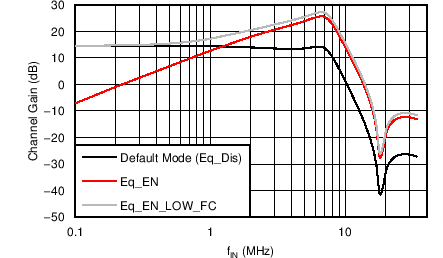
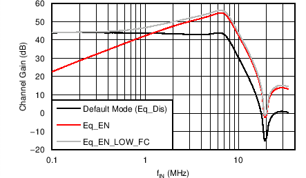
The HPF and LPF cutoff frequencies (of the antialiasing filter) are the same as per the FILTER_BW setting. In this mode, overall channel gain increases by an additional fixed gain of 15 dB from the HPF block. Typical frequency response plots showing different equalizer modes along with the default mode are shown in Figure 7-9 and Figure 7-10.
 Figure 7-9 Filter Response (PGA Gain = 0 dB)
 Figure 7-10 Filter Response (PGA Gain = 30 dB)