SBASB81 December 2024 AFE5401-EP
PRODUCTION DATA
- 1
- 1 Features
- 2 Applications
- 3 Description
- 4 Pin Configuration and Functions
-
5 Specifications
- 5.1 Absolute Maximum Ratings
- 5.2 ESD Ratings
- 5.3 Recommended Operating Conditions
- 5.4 Thermal Information
- 5.5 Electrical Characteristics
- 5.6 Digital Characteristics
- 5.7 Timing Requirements: Output Interface
- 5.8 Timing Requirements: RESET
- 5.9 Timing Requirements: Serial Interface Operation
- 5.10 Typical Characteristics
- 6 Parameter Measurement Information
-
7 Detailed Description
- 7.1 Overview
- 7.2 Functional Block Diagram
- 7.3 Feature Description
- 7.4 Device Functional Modes
- 7.5 Programming
- 7.6 Register Maps
- 8 Application and Implementation
- 9 Revision History
- 10Device and Documentation Support
- 11Mechanical, Packaging, and Orderable Information
パッケージ・オプション
メカニカル・データ(パッケージ|ピン)
- RGC|64
サーマルパッド・メカニカル・データ
- RGC|64
発注情報
7.4.6 Diagnostic Mode
The device offers various diagnostic modes to check proper device operation at a system level. These modes can be enabled using the SPI and the outputs of these modes are stored in diagnostic read-only registers.
- Internal reference status check: In this mode, the on-chip band-gap voltage, ADC reference, and clock generation are verified for functionality. Reading a 0 on these bits indicates that these blocks are functioning properly. The DIAG_MODE_EN register bit must be set to 1. The DIG_REG register bits for this mode are:
- DIG_REG[0] for ADC references,
- DIG_REG[1] for band gap, and
- DIG_REG[2] for clock generation.
- DC input force: In this mode, a dc voltage can be internally forced at the LNA input to test the entire signal chain. During this test, the device analog inputs should be left floating. This mode can be asserted by setting the DC_INP_EN bit to 1 and programming the DC_INP_PROG[0:2] bits. In this mode, the equalizer is disabled internally.
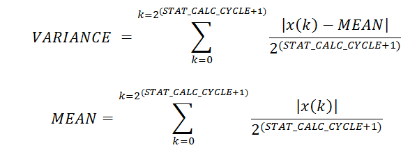
- Variance (noise) and mean measurement: Variance and mean of the ADC output can be analyzed using the on-chip STAT module. The STAT_EN, STAT_CALC_CYCLE, and STAT_CH_SEL, STAT_CH_AUTO_SEL options should be set to compute the variance and mean. These values can be monitored using channel-specific, read-only registers. Alternatively, these values can also be read using HEADER_MODE. Output variance and mean calculation is determined by Equation 3.
Equation 3.

STAT_CALC_CYCLE must be set to a large value to obtain better accuracy. Mean provides the average dc value of the ADC output (mid code). The STAT module integration time is defined by: tAFE_CLK × 2(STAT_CALC_CYCLE+1) when the STAT_CH_SEL option is selected. When STAT_CH_AUTO_SEL is enabled, the STAT module integration time is defined by: 4 × tAFE_CLK × 2(STAT_CALC_CYCLE+1).
- Temperature sensor: The device junction temperature measurement can be enabled and monitored using TEMP_SENS_EN and TEMP_CONV_EN. The temperature output is saved in a diagnostic read-only register, TEMP_DATA. Alternatively, this data can also be read using HEADER_MODE. The TEMP_DATA value is a 9-bit, twos complement data in degrees Celsius. The temperature data is internally updated as per Equation 4:
Equation 4. Temperature Data Update Cycle = 1024 × TAFE_CLK × 16