JAJSVV8 December 2024 AFE5401-EP
PRODUCTION DATA
- 1
- 1 特長
- 2 アプリケーション
- 3 概要
- 4 Pin Configuration and Functions
-
5 Specifications
- 5.1 Absolute Maximum Ratings
- 5.2 ESD Ratings
- 5.3 Recommended Operating Conditions
- 5.4 Thermal Information
- 5.5 Electrical Characteristics
- 5.6 Digital Characteristics
- 5.7 Timing Requirements: Output Interface
- 5.8 Timing Requirements: RESET
- 5.9 Timing Requirements: Serial Interface Operation
- 5.10 Typical Characteristics
- 6 Parameter Measurement Information
-
7 Detailed Description
- 7.1 Overview
- 7.2 Functional Block Diagram
- 7.3 Feature Description
- 7.4 Device Functional Modes
- 7.5 Programming
- 7.6 Register Maps
- 8 Application and Implementation
- 9 Revision History
- 10Device and Documentation Support
- 11Mechanical, Packaging, and Orderable Information
7.3.6 Input Clock Divider
The device clock input is passed through a clock divider block that can divide the input clock by a factor of 1, 2, 3, or 4. This divided clock (AFE_CLK) is used for simultaneously sampling the four ADC inputs. In default mode, a division factor of 1 is used where the AFE_CLK frequency is the same as the input clock frequency. The clock divider block can be enabled using the DIV_EN register bit and, when enabling this bit, the AFE_CLK frequency is automatically determined by the serialization factor set by the CH_OUT_DIS register bits (Table 7-7). The division factor can also be manually specified by enabling the DIV_FRC and DIV_REG register bits. Care must be taken to ensure that the input clock frequency is within the recommended operating range specified in the Section 5.3.
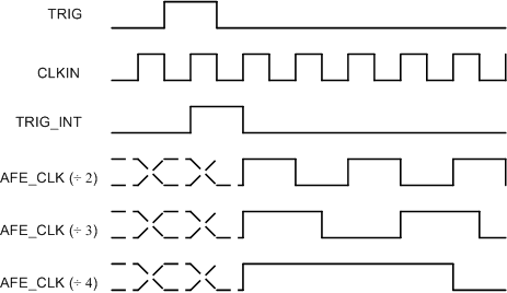
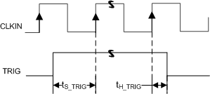
After device reset, the divider is reset at the first pulse applied on the TRIG pin. This configuration is especially useful when using multiple devices in the system, where the sampling instants of all ADCs in the system must be synchronized. Figure 7-5 illustrates the TRIG timing diagram and the various divided-down AFE_CLK signals. Figure 7-6 provides the TRIG input setup and hold time with respect to the device clock input. Bit settings for the DIV_EN register, DIV_FRD register, and DIV_REG register are provided in Table 7-4, Table 7-5, and Table 7-6, respectively.
 Figure 7-5 Input Clock Divider
 Figure 7-6 TRIG CLKIN Setup and Hold
| DIV_EN | DESCRIPTION |
|---|---|
| 0 | Divider disabled and bypassed |
| 1 | Divider enabled |
| DIV_FRC | DESCRIPTION |
|---|---|
| 0 | Input divider ratio = serialization factor(1) (automatically set) |
| 1 | Input divider ratio = DIV_REG (manually set) |
| DIV_REG | DESCRIPTION |
|---|---|
| 0 | Divider disabled and bypassed |
| 1 | Divide-by-2 |
| 2 | Divide-by-3 |
| 3 | Divide-by-4 |