Typical values at TA = +25°C, ADC Sampling Rate = 2949.12 GHz. Default conditions: output sample rate = 491.52 MSPS (decimate by 6), PLL clock mode with fREF = 491.52 MHz, AIN = –3 dBFS, DSA setting = 4 dB.

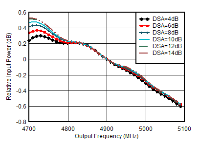
| With
matching, normalized to power at 4.9 GHz for each DSA
setting |
Figure 7-386 RX
Inband Gain Flatness, fIN = 4900 MHz
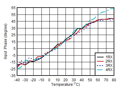
| With
4.9 GHz matching, normalized to phase at 25°C |
|
|
Figure 7-388 RX
Input Phase vs Temperature and DSA at fOUT = 4.9 GHz
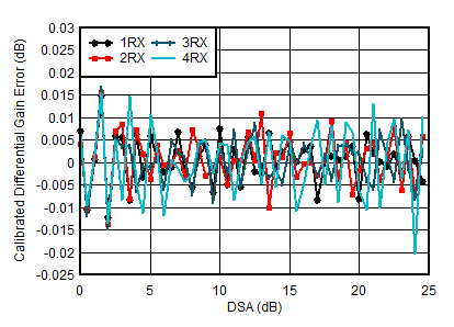
| With
4.9 GHz matching |
| Differential Amplitude Error = PIN(DSA
Setting – 1) – PIN(DSA Setting) + 1 |
Figure 7-390 RX
Calibrated Differential Amplitude Error vs DSA Setting at 4.9 GHz
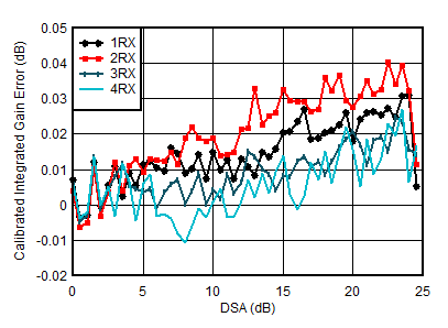
| With
4.9 GHz matching |
| Integrated Amplitude Error = PIN(DSA
Setting) – PIN(DSA Setting = 0) + (DSA
Setting) |
Figure 7-392 RX
Calibrated Integrated Amplitude Error vs DSA Setting at 4.9 GHz
| With
4.9 GHz matching |
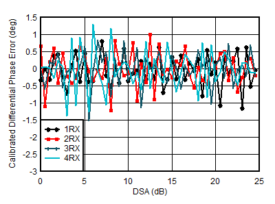
| Differential Phase Error = PhaseIN(DSA
Setting – 1) – PhaseIN(DSA Setting) |
Figure 7-394 RX
Calibrated Differential Phase Error vs DSA Setting at 4.9 GHz
| With
4.9 GHz matching |
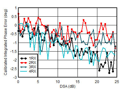
| Integrated Phase Error = Phase(DSA Setting) – Phase(DSA
Setting = 0) |
Figure 7-396 RX
Calibrated Integrated Phase Error vs DSA Setting at 4.9 GHz
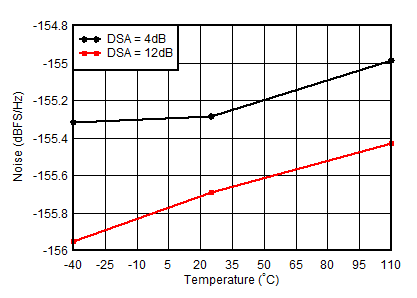
| With
4.9 GHz matching, 12.5-MHz offset from tone |
|
Figure 7-398 RX
Noise Spectral Density vs Temperature at 4.9 GHz
| With
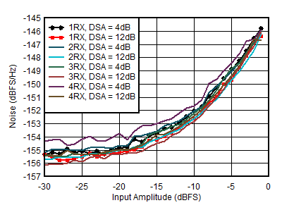
4.9 GHz matching, 12.5-MHz offset from tone |
|
Figure 7-400 RX
Noise Spectral Density vs Input Amplitude and Channel at 4.9 GHz
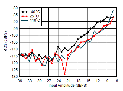
| With
4.9 GHz matching, tone spacing = 20 MHz, DSA = 4
dB |
|
Figure 7-402 RX
IMD3 vs Input Level and Temperature at 4.9 GHz
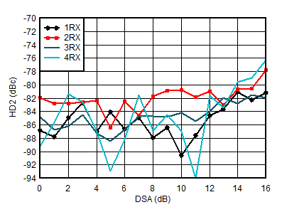
| With
4.9 GHz matching, measured after HD2 trim, DDC bypass
mode (TI only mode for characterization) |
Figure 7-404 RX
HD2 vs DSA Setting and Channel at 4.9 GHz
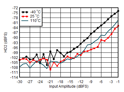
| With
4.9 GHz matching, measured after HD2 trim, DDC bypass
mode (TI only mode for characterization) |
Figure 7-406 RX
HD2 vs Input Level and Temperature at 4.9 GHz
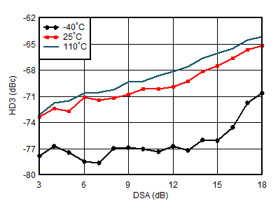
| With
4.9 GHz matching, DDC bypass mode (TI only mode for
characterization) |
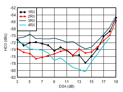
Figure 7-408 RX
HD3 vs DSA Setting and Temperature at 4.9 GHz
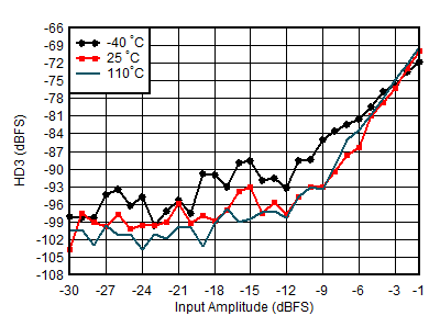
| With
4.9 GHz matching, DDC bypass mode (TI only mode for
characterization) |
Figure 7-410 RX
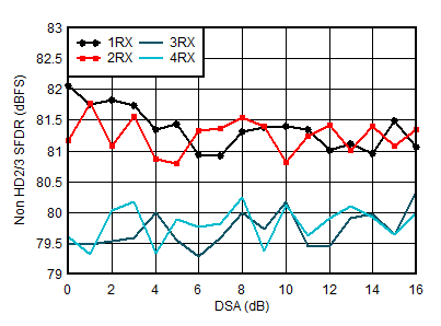
HD3 vs Input Level and Temperature at 4.9 GHz Figure 7-412 RX
Non-HD2/3 vs DSA Setting at 4.9 GHz
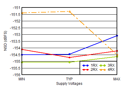
| With
4.9 GHz matching, 12.5-MHz offset, all supplies at MIN,
TYP, or MAX recommended operating voltages |
|
Figure 7-414 RX
Noise Spectral Density vs Supply and Channel at 4.9 GHz
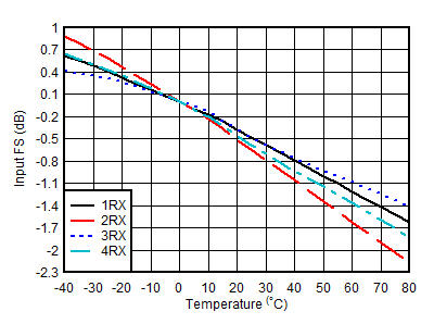
| With
4.9 GHz matching, normalized to fullscale at 25°C for
each channel |
Figure 7-387 RX
Input Fullscale vs Temperature and Channel at 4.9 GHz
| With
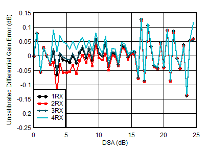
4.9 GHz matching |
| Differential Amplitude Error = PIN(DSA
Setting – 1) – PIN(DSA Setting) + 1 |
Figure 7-389 RX
Uncalibrated Differential Amplitude Error vs DSA Setting at 4.9 GHz
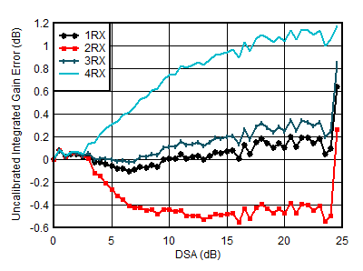
| With
4.9 GHz matching |
| Integrated Amplitude Error = PIN(DSA
Setting) – PIN(DSA Setting = 0) + (DSA
Setting) |
Figure 7-391 RX
Uncalibrated Integrated Amplitude Error vs DSA Setting at 4.9 GHz
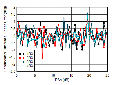
| With
4.9 GHz matching |
| Differential Phase Error = PhaseIN(DSA
Setting – 1) – PhaseIN(DSA Setting) |
Figure 7-393 RX
Uncalibrated Differential Phase Error vs DSA Setting at 4.9 GHz
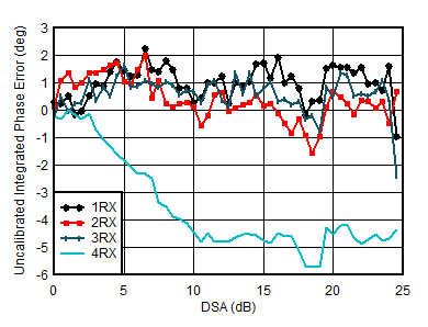
| With
4.9 GHz matching |
| Integrated Phase Error = Phase(DSA Setting) – Phase(DSA
Setting = 0) |
Figure 7-395 RX
Uncalibrated Integrated Phase Error vs DSA Setting at 4.9 GHz
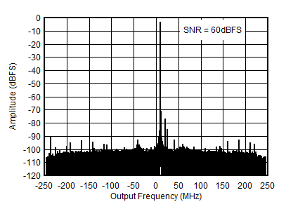
| With
4.9 GHz matching, fIN = 4910 MHz,
AIN= –3 dBFS |
|
|
Figure 7-397 RX
Output FFT at 4.9 GHz
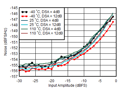
| With
4.9 GHz matching, DSA Setting = 12 dB, 12.5-MHz offset
from tone |
Figure 7-399 RX
Noise Spectral Density vs Input Amplitude and Temperature at 4.9 GHz
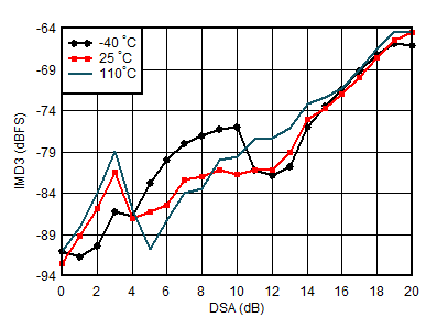
| With
4.9 GHz matching, each tone –7 dBFS, tone spacing = 20
MHz |
Figure 7-401 RX
IMD3 vs DSA Setting and Temperature at 4.9 GHz
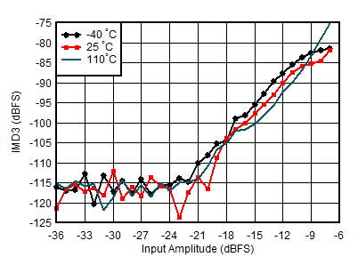
| With
4.9 GHz matching, tone spacing = 20 MHz, DSA = 12
dB |
Figure 7-403 RX
IMD3 vs Input Level and Temperature at 4.9 GHz
| With
4.9 GHz matching, measured after HD2 trim, DDC bypass
mode (TI only mode for characterization) |
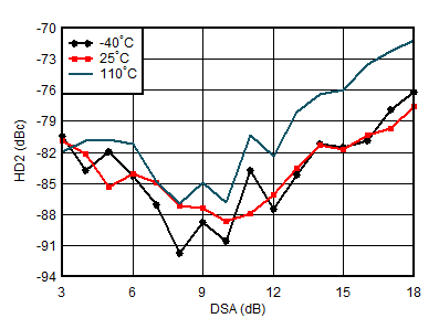
Figure 7-405 RX
HD2 vs DSA and Temperature at 4.9 GHz
| With
4.9 GHz matching, DDC bypass mode (TI only mode for
characterization) |
Figure 7-407 RX
HD3 vs DSA Setting and Channel at 4.9 GHz
| With
4.9 GHz matching, DDC bypass mode (TI only mode for
characterization) |
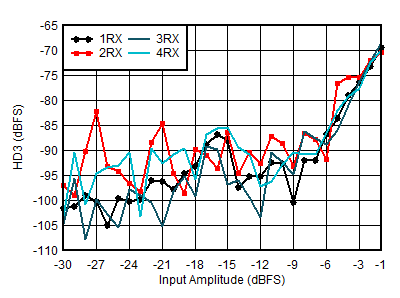
Figure 7-409 RX
HD3 vs Input Level and Channel at 4.9 GHz
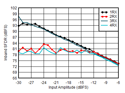
| With
4.9 GHz matching, decimate by 3 |
Figure 7-411 RX
In-Band SFDR (±400 MHz) vs Input Amplitude and Channel at 4.9 GHz
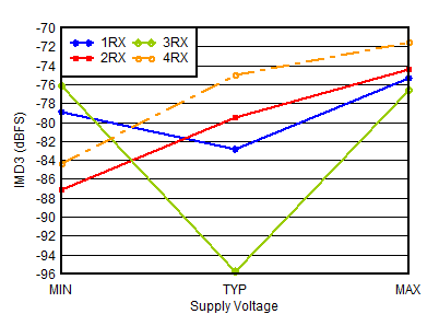
| With
4.9 GHz matching, –7 dBFS each tone, 20-MHz tone
spacing, all supplies at MIN, TYP, or MAX recommended
operating voltages |
Figure 7-413 RX
IMD3 vs Supply and Channel at 4.9 GHz