JAJSP50A May 2023 – September 2023 AMC131M03-Q1
PRODUCTION DATA
- 1
- 1 特長
- 2 アプリケーション
- 3 概要
- 4 Revision History
- 5 Pin Configuration and Functions
-
6 Specifications
- 6.1 Absolute Maximum Ratings
- 6.2 ESD Ratings
- 6.3 Recommended Operating Conditions
- 6.4 Thermal Information
- 6.5 Insulation Specifications
- 6.6 Safety-Related Certifications
- 6.7 Safety Limiting Values
- 6.8 Electrical Characteristics
- 6.9 Timing Requirements
- 6.10 Switching Characteristics
- 6.11 Timing Diagrams
- 6.12 Typical Characteristics
- 7 Parameter Measurement Information
-
8 Detailed Description
- 8.1 Overview
- 8.2 Functional Block Diagram
- 8.3
Feature Description
- 8.3.1 Isolated DC/DC Converter
- 8.3.2 High-Side Current Drive Capability
- 8.3.3 Isolation Channel Signal Transmission
- 8.3.4 Input ESD Protection Circuitry
- 8.3.5 Input Multiplexer
- 8.3.6 Programmable Gain Amplifier (PGA)
- 8.3.7 Voltage Reference
- 8.3.8 Internal Test Signals
- 8.3.9 Clocking and Power Modes
- 8.3.10 ΔΣ Modulator
- 8.3.11 Digital Filter
- 8.3.12 Channel Phase Calibration
- 8.3.13 Calibration Registers
- 8.3.14 Register Map CRC
- 8.3.15 Temperature Sensor
- 8.3.16 General-Purpose Digital Output (GPO)
- 8.4 Device Functional Modes
- 8.5
Programming
- 8.5.1
Serial Interface
- 8.5.1.1 Chip Select (CS)
- 8.5.1.2 Serial Data Clock (SCLK)
- 8.5.1.3 Serial Data Input (DIN)
- 8.5.1.4 Serial Data Output (DOUT)
- 8.5.1.5 Data Ready (DRDY)
- 8.5.1.6 Conversion Synchronization or System Reset (SYNC/RESET)
- 8.5.1.7 SPI Communication Frames
- 8.5.1.8 SPI Communication Words
- 8.5.1.9 Short SPI Frames
- 8.5.1.10 Communication Cyclic Redundancy Check (CRC)
- 8.5.1.11 SPI Timeout
- 8.5.2 ADC Conversion Data
- 8.5.3 Commands
- 8.5.4 ADC Output Buffer and FIFO Buffer
- 8.5.5 Collecting Data for the First Time or After a Pause in Data Collection
- 8.5.1
Serial Interface
- 8.6 AMC131M03-Q1 Registers
- 9 Application and Implementation
- 10Device and Documentation Support
- 11Mechanical, Packaging, and Orderable Information
9.2.3 Application Curves
Electromagnetic interference (EMI) testing is common in many applications using the AMC131M03-Q1 to verify the system does not produce radiated emissions that exceed the defined levels that can possibly negatively impact other components or circuits in the system. See the Understanding electromagnetic compliance tests in digital isolators white paper for a more in-depth description of EMI. The magnitude of acceptable radiation and testing procedure for radiated emissions is put in place by the Comité International Spécial des Perturbations Radio, also known as CISPR. Industrial applications measure according to the CISPR 11 standard, and automotive applications measure to the CISPR 25 standard. For more information on the CISPR standards and the respective magnitudes over frequency, see the An overview of radiated EMI specifications for power supplies white paper.
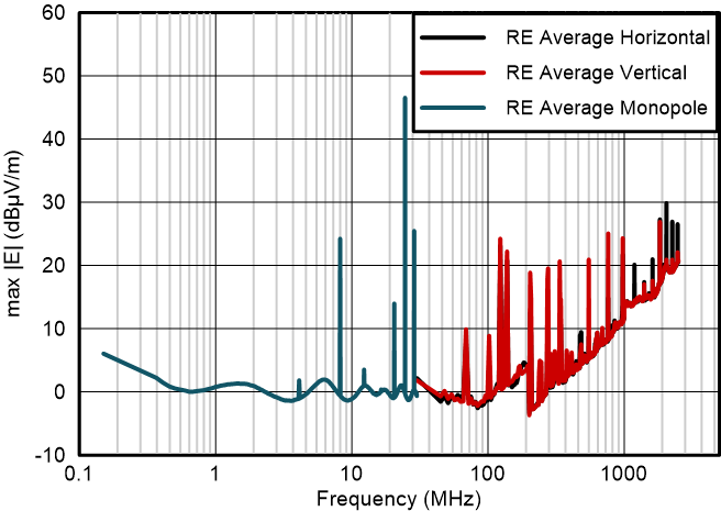
Figure 9-5 shows the radiated emissions measurement for the AMC131M03-Q1 using the evaluation module available at AMC131M03EVM. Because the evaluation module is designed for ease of use and evaluating ADC performance, there is room for improvement in terms of radiated emissions. The evaluation module includes both a clocking and a flip-flop circuit for choosing which clock frequency to not include in a realistic design. Also, the board has two layers. However, in an EMI optimized design, a four-layer design with GND layers on the top and bottom for the primary (low-side) portion of the PCB and digital signals on the internal layers improves results.
The measurements were done following CISPR 25 requirements, in a in a semi-anechoic chamber using linearly polarized electric field antennas configured for horizontal and vertical polarizations with a 1-meter distance. The ADC is receiving a continuous clock at the CLKIN pin, and is generating conversion results, however there is no SPI communication while the emission profile is characterized.
A vertically mounted active monopole rod antenna with counterpoise was used for low-frequency measurements from 150 kHz to 30 MHz. A biconical antenna was used for the range of 30 MHz to 200 MHz (horizontal and vertical), and a log-periodic dipole array (LPDA) antenna was used for the frequency range of 200 MHz to 1 GHz (horizontal and vertical). A dual-ridge-horn antenna (DRHA) was used from 1 GHz to 2.5 GHz (horizontal and vertical).
 Figure 9-5 AMC131M03-Q1 Radiated Emission CISPR25
Measurement