JAJSPF2A june 2023 – august 2023 AMC3311
PRODUCTION DATA
- 1
- 1 特長
- 2 アプリケーション
- 3 概要
- 4 Revision History
- 5 Pin Configuration and Functions
-
6 Specifications
- 6.1 Absolute Maximum Ratings
- 6.2 ESD Ratings
- 6.3 Recommended Operating Conditions
- 6.4 Thermal Information
- 6.5 Power Ratings
- 6.6 Insulation Specifications
- 6.7 Safety-Related Certifications
- 6.8 Safety Limiting Values
- 6.9 Electrical Characteristics
- 6.10 Switching Characteristics
- 6.11 Timing Diagram
- 6.12 Insulation Characteristics Curves
- 6.13 Typical Characteristics
- 7 Detailed Description
- 8 Application and Implementation
- 9 Device and Documentation Support
- 10Mechanical, Packaging, and Orderable Information
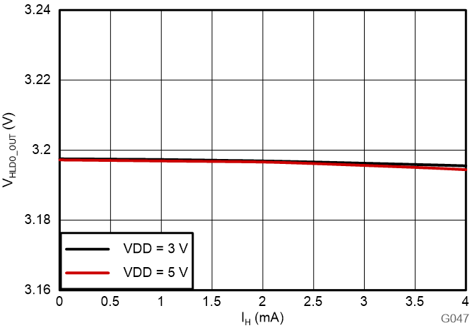
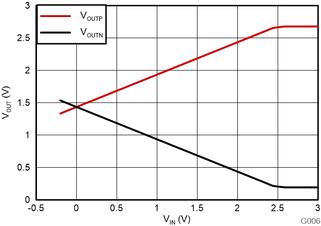
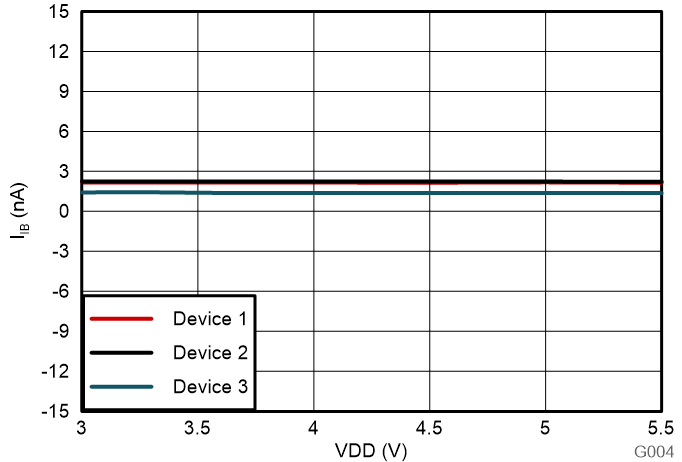
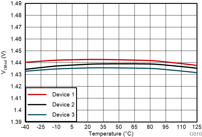
6.13 Typical Characteristics
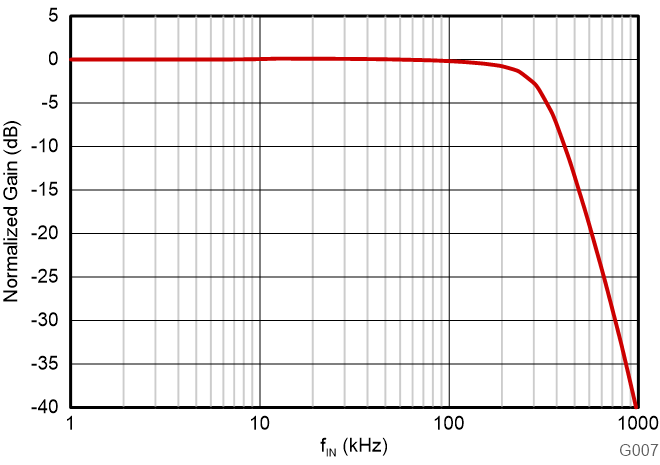
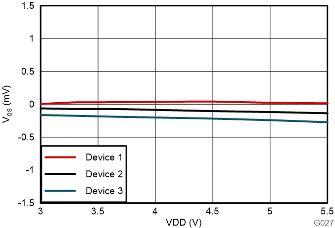
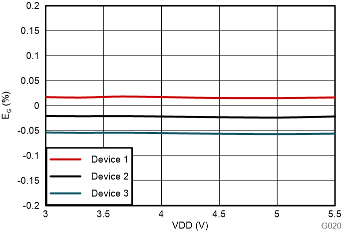
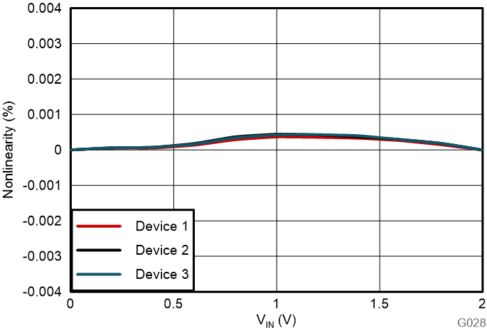
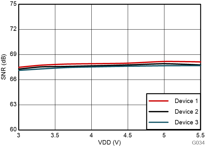
at VDD = 3.3 V, IN = 0 V to 2 V, and fIN = 10 kHz (unless otherwise noted)

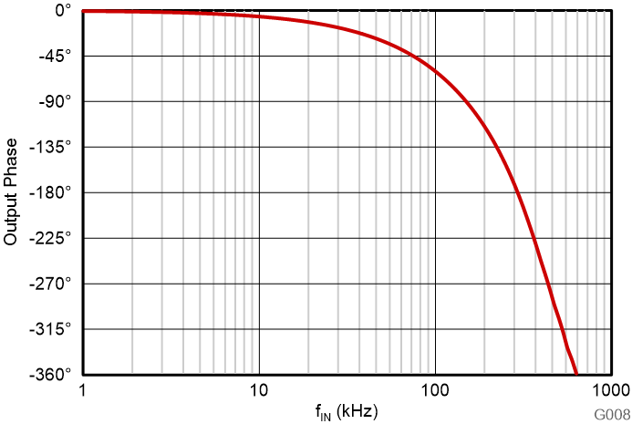


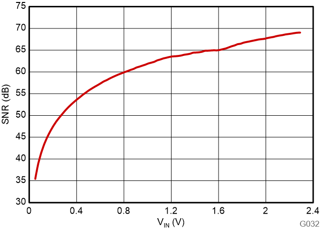

| VIN = 2 V |


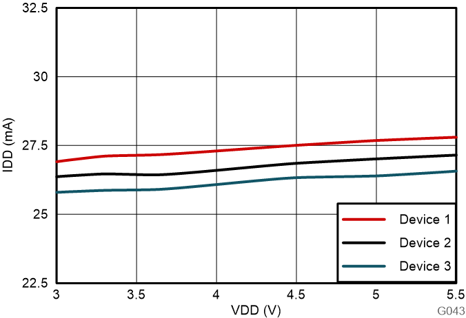
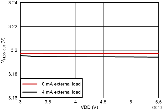
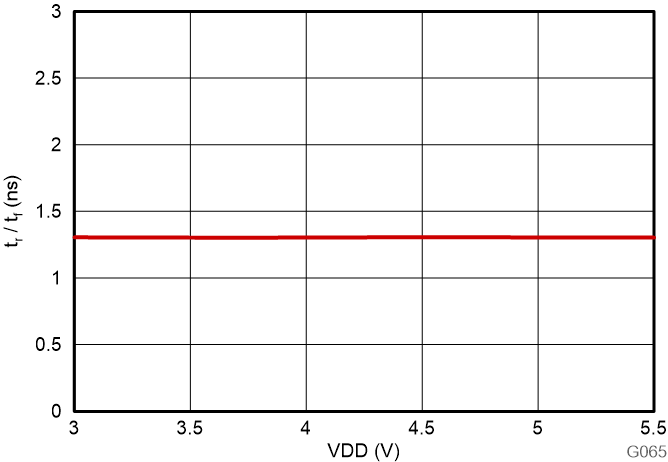
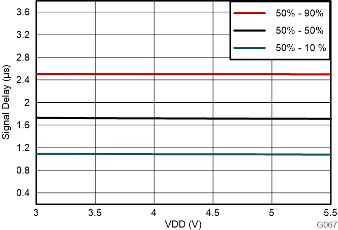

| Total uncalibrated output error is defined as: (VOUT – VIN × G) / (VClipping × G), where G is the nominal gain of the device (1 V/V) and VClipping is 2.516 V |
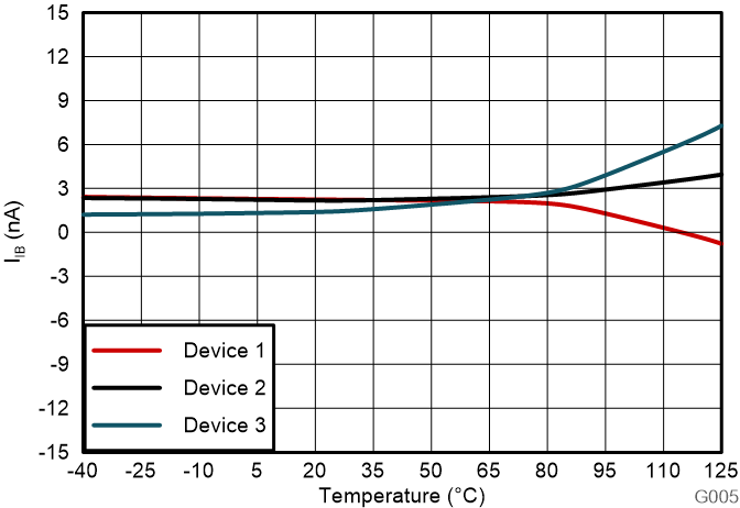
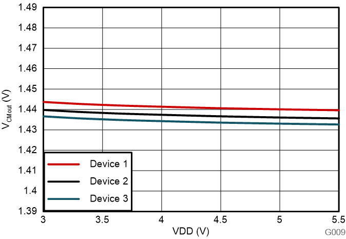


| VIN = 2 V |


