JAJSPB8A June   2009  – January 2023 AMC6821-Q1

PRODUCTION DATA  

  1. 特長
  2. アプリケーション
  3. 概要
  4. Revision History
  5. 概要 (続き)
  6. Pin Configuration and Functions
  7. Specifications
    1. 7.1 Absolute Maximum Ratings
    2. 7.2 ESD Ratings
    3. 7.3 Recommended Operating Conditions
    4. 7.4 Thermal Information
    5. 7.5 Electrical Characteristics
    6. 7.6 Timing Requirements
    7. 7.7 Typical Characteristics
  8. Detailed Description
    1. 8.1 Functional Block Diagram
    2. 8.2 Feature Description
      1. 8.2.1 ADC Converter
      2. 8.2.2 Temperature Sensor
        1. 8.2.2.1 Series Resistance Cancellation
        2. 8.2.2.2 Reading Temperature Data
        3. 8.2.2.3 Temperature Out-of-Range Detection
        4. 8.2.2.4 Remote Temperature Sensor Failure Detection
      3. 8.2.3 PWM Output
      4. 8.2.4 PWM Waveform Setting
      5. 8.2.5 Fan Speed Measurement
        1. 8.2.5.1 Tach-Data Register
          1. 8.2.5.1.1 Reading the Tach Data Register
          2. 8.2.5.1.2 RPM Measurement Rate
          3. 8.2.5.1.3 Select Number of Pulses/Revolution
          4. 8.2.5.1.4 Tach Mode Selection
          5. 8.2.5.1.5 Fan RPM Out-of-Range Detection
      6. 8.2.6 Fan Failure Detection
      7. 8.2.7 FAN-FAULT Pin
      8. 8.2.8 Fan Control
        1. 8.2.8.1 THERM Pin and External Hardware Control
          1. 8.2.8.1.1 THERM Pin as an Output
          2. 8.2.8.1.2 THERM Pin as an Input
        2. 8.2.8.2 Fan Spin-Up
        3. 8.2.8.3 Normal Fan Speed Control
          1. 8.2.8.3.1 Software DCY Control Mode
          2. 8.2.8.3.2 Software-RPM Control Mode (Fan Speed Regulator)
          3. 8.2.8.3.3 Auto Temperature Fan Mode
      9. 8.2.9 Interrupt
        1. 8.2.9.1 OVR Pin
        2. 8.2.9.2 SMBALERT Pin
        3. 8.2.9.3 SMBALERT Interrupt Behavior
        4. 8.2.9.4 Handling SMBALERT Interrupts
    3. 8.3 Device Functional Modes
    4. 8.4 Programming
      1. 8.4.1 SMBus Interface
        1. 8.4.1.1 Communication Protocols
      2. 8.4.2 SMBus Alert Response Address (ARA)
      3. 8.4.3 Power-On Reset and Start Operation
    5. 8.5 Register Map
      1. 8.5.1 Register Description
        1. 8.5.1.1 Device Configuration Registers
        2. 8.5.1.2 Device Status Registers
        3. 8.5.1.3 Fan Controller Registers
        4. 8.5.1.4 Temperature Data Registers
        5. 8.5.1.5 Temperature Limit Registers
          1. 8.5.1.5.1 Tach-Data Register
          2. 8.5.1.5.2 Tach Setting Register
          3. 8.5.1.5.3 Tach Low Limit Register
          4. 8.5.1.5.4 Tach High Limit Register
  9. Application and Implementation
    1. 9.1 Power Supply Recommendations
  10. 10Device and Documentation Support
    1. 10.1 ドキュメントの更新通知を受け取る方法
    2. 10.2 サポート・リソース
    3. 10.3 Trademarks
    4. 10.4 静電気放電に関する注意事項
    5. 10.5 用語集
  11. 11Mechanical, Packaging, and Orderable Information

パッケージ・オプション

メカニカル・データ(パッケージ|ピン)
サーマルパッド・メカニカル・データ
発注情報
Tach Mode Selection

The TACH-MODE bit of Configuration Register 2 specifies the TACH pulse output mode of the fan. Some fans (such as three- and two-wire) are powered directly by the PWM, and must be PWM-On to provide a TACH pulse output. When the PWM-Out pin switches these fans ON/OFF directly, the PWM-Out must be kept ON to power the fan during the measurement. In this case, the TACH-MODE bit of Configuration Register 2 must be cleared ('0'). When TACH-MODE = 0, the PWM-Out pin is kept ON during the critical tach edges of the measurement period. Clearing the TACH mode ('0') also enables the internal correction circuitry to correct the error caused by the extra duty cycle applied in the measurement period. The power-on default value of the PWM mode is '0'.
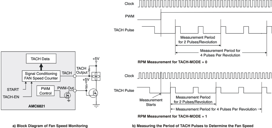
GUID-A928B941-54F9-483E-BE76-900AF7720759-low.gifFigure 8-7 Fan Speed Measurement

Some fans (such as the JMC® four-wire fan) are powered directly by dc power, instead of being powered by the PWM. In this case, the TACH mode must be set to '1'. When TACH-MODE = 1, the PWM-Out pin is not forced ON; instead, the status is controlled completely by the DCY register, just as in normal operation. Setting TACH-MODE to '1' also disables the internal correction circuit because no extra duty cycle is applied. Setting the TACH mode to '1' allows TACH reading continuously, regardless of the status of the PWM-Out pin.

The selection of the TACH mode affects the RPM monitoring and control. When the TACH-MODE bit is equal to '1', the duty cycle of the PWM-Out pin is always determined by the calculated value; the TACH data are always updated at every RPM monitoring. However, when the TACH-MODE bit is equal to '0', in the Software-RPM Control mode the PWM-Out pin is forced to 30% if the calculated duty cycle is less than 30%; in other modes, the PWM-Out pin is forced to 0% and the TACH data are not updated if the calculated duty cycle is less than 7%.