JAJSPK3G May 2001 – December 2022 BQ2057C
PRODUCTION DATA
- 1 特長
- 2 アプリケーション
- 3 概要
- 4 Revision History
- 5 概要 (続き)
- 6 Device Comparison Table
- 7 Pin Configuration and Functions
- 8 Specifications
- 9 Detailed Description
-
10Application and Implementation
- 10.1
Application Information
- 10.1.1 Functional Description
- 10.1.2 Qualification and Precharge
- 10.1.3 Current Regulation Phase
- 10.1.4 Voltage Regulation Phase
- 10.1.5 Charge Termination and Recharge
- 10.1.6 Battery Temperature Monitoring
- 10.1.7 Charge Inhibit Function
- 10.1.8 Charge Status Indication
- 10.1.9 Low-power Sleep Mode
- 10.1.10 Selecting an External Pass-Transistor
- 10.1.11 Selecting Input Capacitor
- 10.1.12 Selecting Output Capacitor
- 10.1.13 Automatic Charge-rate Compensation
- 10.2 Typical Application
- 10.1
Application Information
- 11Power Supply Recommendations
- 12Layout
- 13Device and Documentation Support
- 14Mechanical, Packaging, and Orderable Information
パッケージ・オプション
デバイスごとのパッケージ図は、PDF版データシートをご参照ください。
メカニカル・データ(パッケージ|ピン)
- D|8
- DGK|8
- PW|8
サーマルパッド・メカニカル・データ
発注情報
10.1.6 Battery Temperature Monitoring
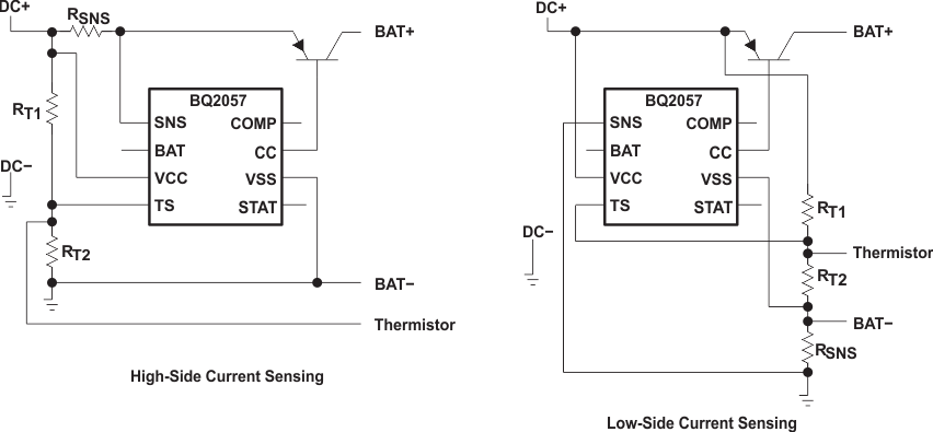
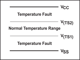
The BQ2057 continuously monitors temperature by measuring the voltage between the TS and VSS pins. A negative- or a positive-temperature coefficient thermistor (NTC, PTC) and an external voltage divider typically develop this voltage. (See Figure 10-9.) The BQ2057 compares this voltage against its internal V(TS1) and V(TS2) thresholds to determine if charging is allowed. (See Figure 10-10.) The temperature sensing circuit is immune to any fluctuation in VCC, since both the external voltage divider and the internal thresholds (V(TS1) and V(TS2)) are referenced to VCC.
The resistor values of R(T1) and R(T2) are calculated by the following equations:
For NTC Thermistors


For PTC Thermistors


Where R(TC) is the cold temperature resistance and R(TH) is the hot temperature resistance of thermistor, as specified by the thermistor manufacturer.
RT1 or RT2 can be omitted If only one temperature (hot or cold) setting is required. Applying a voltage between the V(TS1) and V(TS2) thresholds to pin TS disables the temperature-sensing feature.
 Figure 10-9 Temperature Sensing Circuits
 Figure 10-10 BQ2057 TS
Input Thresholds