JAJSPK3G May 2001 – December 2022 BQ2057C
PRODUCTION DATA
- 1 特長
- 2 アプリケーション
- 3 概要
- 4 Revision History
- 5 概要 (続き)
- 6 Device Comparison Table
- 7 Pin Configuration and Functions
- 8 Specifications
- 9 Detailed Description
-
10Application and Implementation
- 10.1
Application Information
- 10.1.1 Functional Description
- 10.1.2 Qualification and Precharge
- 10.1.3 Current Regulation Phase
- 10.1.4 Voltage Regulation Phase
- 10.1.5 Charge Termination and Recharge
- 10.1.6 Battery Temperature Monitoring
- 10.1.7 Charge Inhibit Function
- 10.1.8 Charge Status Indication
- 10.1.9 Low-power Sleep Mode
- 10.1.10 Selecting an External Pass-Transistor
- 10.1.11 Selecting Input Capacitor
- 10.1.12 Selecting Output Capacitor
- 10.1.13 Automatic Charge-rate Compensation
- 10.2 Typical Application
- 10.1
Application Information
- 11Power Supply Recommendations
- 12Layout
- 13Device and Documentation Support
- 14Mechanical, Packaging, and Orderable Information
パッケージ・オプション
デバイスごとのパッケージ図は、PDF版データシートをご参照ください。
メカニカル・データ(パッケージ|ピン)
- D|8
- DGK|8
- PW|8
サーマルパッド・メカニカル・データ
発注情報
10.1.3 Current Regulation Phase
The BQ2057 regulates current while the battery-pack voltage is less than the regulation voltage, VO(REG). The BQ2057 monitors charge current at the SNS input by the voltage drop across a sense-resistor, RSNS, in series with the battery pack. In high-side current sensing configuration (see Figure 10-5), RSNS is between the VCC and SNS pins, and in low-side sensing (see Figure 10-6) the RSNS is between VSS (battery negative) and SNS (charger ground) pins. Charge-current feedback, applied through pin SNS, maintains a voltage of V(SNS) across the current sense resistor. Equation 1 calculates the value of the sense resistor:
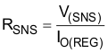
Where IO(REG) is the desired charging current.
 Figure 10-5 High-Side Current Sensing
 Figure 10-6 Low-Side Current Sensing