JAJSPK3G May 2001 – December 2022 BQ2057C
PRODUCTION DATA
- 1 特長
- 2 アプリケーション
- 3 概要
- 4 Revision History
- 5 概要 (続き)
- 6 Device Comparison Table
- 7 Pin Configuration and Functions
- 8 Specifications
- 9 Detailed Description
-
10Application and Implementation
- 10.1
Application Information
- 10.1.1 Functional Description
- 10.1.2 Qualification and Precharge
- 10.1.3 Current Regulation Phase
- 10.1.4 Voltage Regulation Phase
- 10.1.5 Charge Termination and Recharge
- 10.1.6 Battery Temperature Monitoring
- 10.1.7 Charge Inhibit Function
- 10.1.8 Charge Status Indication
- 10.1.9 Low-power Sleep Mode
- 10.1.10 Selecting an External Pass-Transistor
- 10.1.11 Selecting Input Capacitor
- 10.1.12 Selecting Output Capacitor
- 10.1.13 Automatic Charge-rate Compensation
- 10.2 Typical Application
- 10.1
Application Information
- 11Power Supply Recommendations
- 12Layout
- 13Device and Documentation Support
- 14Mechanical, Packaging, and Orderable Information
パッケージ・オプション
デバイスごとのパッケージ図は、PDF版データシートをご参照ください。
メカニカル・データ(パッケージ|ピン)
- D|8
- DGK|8
- PW|8
サーマルパッド・メカニカル・データ
発注情報
10.1.10 Selecting an External Pass-Transistor
The BQ2057 is designed to work with both PNP transistor and P-channel MOSFET. The device should be chosen to handle the required power dissipation, given the circuit parameters, PCB layout and heat sink configuration. The following examples illustrate the design process for either device:
PNP transistor: Selection steps for a PNP bipolar transistor: Example: VI = 4.5 V, I(REG) = 1 A, 4.2-V single-cell Li-Ion (bq2057C). VI is the input voltage to the charger and I(REG) is the desired charge current (see Figure 10-1).
- Determine the maximum power dissipation, PD, in the transistor. The worst case power dissipation happens when the cell voltage, V(BAT), is at its lowest (typically 3 V at the beginning of current regulation phase) and VI is at its maximum.
Where VCS is the voltage drop across the current sense resistor.Equation 7.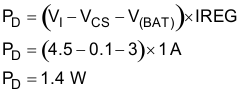
- Determine the package size needed in order to
keep the junction temperature below the manufacturer’s recommended value,
T(J)max. Calculate the total theta, θ(°C/W), needed.
Equation 8.
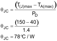
Now choose a device package with a theta at least 10% below this value to account for additional thetas other than the device. A SOT223 package, for instance, has typically a theta of 60°C/W.
- Select a collector-emitter voltage, V(CE), rating greater than the maximum input voltage. A 15-V device will be adequate in this example.
- Select a device that has at least 50% higher drain current IC rating than the desired charge current I(REG).
- Using Equation 9, calculate the minimum beta (β or hFE) needed:
Equation 9.
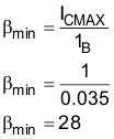
where Imax(C) is the maximum collector current (in this case same as I(REG)), and IB is the base current (chosen to be 35 mA in this example).
The beta of a transistor drops off by a factor of 3 over temperature and also drops off with load. Therefore, note the beta of device at I(REG) and the minimum ambient temperature when choosing the device. This beta should be larger than the minimum required beta.
Now choose a PNP transistor that is rated for V(CE) ≥15 V, θJC ≤ 78°C/W, IC ≥ 1.5 A, βmin ≥ 28 and that is in a SOT223 package.
P-channel MOSFET: Selection steps for a P-channel MOSFET: Example: VI = 5.5 V, I(REG) = 500 mA, 4.2-V single-cell Li-Ion (BQ2057C). VI is the input voltage to the charger and I(REG) is the desired charge current. (See Figure 10-4.)
- Determine the maximum power dissipation, PD, in the transistor.
The worst case power dissipation happens when the cell voltage, V(BAT), is at its lowest (typically 3 V at the beginning of current regulation phase) and VI is at its maximum.
Where VD is the forward voltage drop across the reverse-blocking diode (if one is used), and VCS is the voltage drop across the current sense resistor.Equation 10.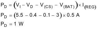
- Determine the package size needed in order to
keep the junction temperature below the manufacturer’s recommended value,
TJMAX. Calculate the total theta, θ(°C/W), needed.
Equation 11.
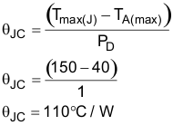
Now choose a device package with a theta at least 10% below this value to account for additional thetas other than the device. A TSSOP-8 package, for instance, has typically a theta of 70°C/W.
- Select a drain-source voltage, V(DS), rating greater than the maximum input voltage. A 12-V device will be adequate in this example.
- Select a device that has at least 50% higher drain current (ID) rating than the desired charge current I(REG).
- Verify that the available drive is large enough
to supply the desired charge current. Equation 12.
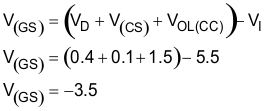
Where V(GS) is the gate-to-source voltage, VD is the forward voltage drop across the reverse-blocking diode (if one is used), and VCS is the voltage drop across the current sense resistor, and VOL(CC) is the CC pin output low voltage specification for the BQ2057.
Select a MOSFET with gate threshold voltage, V(GSth), rating less than the calculated V(GS).
Now choose a P-channel MOSFET transistor that is rated for VDS ≤ −15 V, θJC ≤ 110°C/W, ID ≥ 1 A, V(GSth) ≥ −3.5 V and in a TSSOP package.