JAJSL78D september 2009 – may 2021 BQ24050 , BQ24052
PRODUCTION DATA
- 1
- 1 特長
- 2 アプリケーション
- 3 概要
- 4 Revision History
- 5 Pin Configuration and Functions
-
6 Specifications
- 6.1 Absolute Maximum Ratings #GUID-2D40D94D-8E9B-4250-B39D-57145C9518DB/SLUS9405873
- 6.2 ESD Ratings
- 6.3 Recommended Operating Conditions #GUID-C5354C38-DF78-4F74-91ED-68706C55D3F9/SLUS9401392
- 6.4 Thermal Information
- 6.5 Electrical Characteristics
- 6.6 Timing Requirements
- 6.7 Switching Characteristics
- 6.8 Typical Characteristics
-
7 Detailed Description
- 7.1 Overview
- 7.2 Functional Block Diagram
- 7.3
Feature Description
- 7.3.1 Power Down, or Undervoltage Lockout (UVLO)
- 7.3.2 Power Up
- 7.3.3 D+, D– Detection
- 7.3.4 New Charge Cycle
- 7.3.5 Overvoltage Protection (OVP) – Continuously Monitored
- 7.3.6 CHG Pin Indication
- 7.3.7 CHG LED Pullup Source
- 7.3.8 Input DPM Mode (VIN-DPM or IN-DPM)
- 7.3.9 OUT
- 7.3.10 ISET
- 7.3.11 TS
- 7.3.12 Termination and Timer Disable Mode (TTDM) -TS Pin High
- 7.3.13 Timers
- 7.3.14 Termination
- 7.3.15 Battery Detect Routine
- 7.3.16 Refresh Threshold
- 7.3.17 Starting a Charge on a Full Battery
- 7.4 Device Functional Modes
- 7.5 Programming
- 8 Application and Implementation
- 9 Power Supply Recommendations
- 10Layout
- 11Device and Documentation Support
- Mechanical, Packaging, and Orderable Information
7.3.10 ISET
An external resistor is used to Program the Output Current (10 mA to 1.0 A) and can be used as a current monitor.
Where:
IOUT is the desired fast charge current;
KISET is a gain factor found in the electrical specification
For greater accuracy at lower currents, part of the sense FET is disabled to give better resolution. Figure 6-12 shows the transition from low current to higher current. Going from higher currents to low currents, there is hysteresis and the transition occurs around 0.15 A.
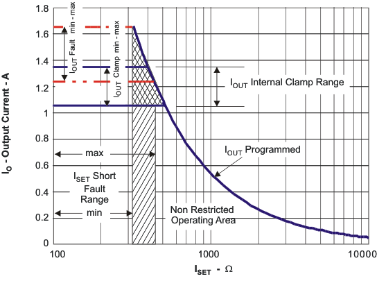
The ISET resistor is short protected and will detect a resistance lower than ≉340 Ω. The detection requires at least 80 mA of output current. If a “short” is detected, then the IC will latch off and can only be reset by cycling the power. The OUT current is internally clamped to a maximum current between 1.05 A and 1.4 A and is independent of the ISET short detection circuitry, as shown in Figure 7-5. Also, see Figure 8-2 and Figure 6-8.
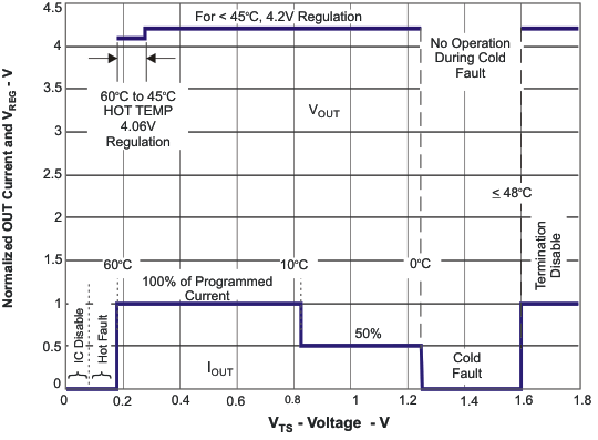
 Figure 7-4 Operation Over TS Bias Voltage
  Figure 7-5 Programmed / Clamped Out Current