JAJSL78D september 2009 – may 2021 BQ24050 , BQ24052
PRODUCTION DATA
- 1
- 1 特長
- 2 アプリケーション
- 3 概要
- 4 Revision History
- 5 Pin Configuration and Functions
-
6 Specifications
- 6.1 Absolute Maximum Ratings #GUID-2D40D94D-8E9B-4250-B39D-57145C9518DB/SLUS9405873
- 6.2 ESD Ratings
- 6.3 Recommended Operating Conditions #GUID-C5354C38-DF78-4F74-91ED-68706C55D3F9/SLUS9401392
- 6.4 Thermal Information
- 6.5 Electrical Characteristics
- 6.6 Timing Requirements
- 6.7 Switching Characteristics
- 6.8 Typical Characteristics
-
7 Detailed Description
- 7.1 Overview
- 7.2 Functional Block Diagram
- 7.3
Feature Description
- 7.3.1 Power Down, or Undervoltage Lockout (UVLO)
- 7.3.2 Power Up
- 7.3.3 D+, D– Detection
- 7.3.4 New Charge Cycle
- 7.3.5 Overvoltage Protection (OVP) – Continuously Monitored
- 7.3.6 CHG Pin Indication
- 7.3.7 CHG LED Pullup Source
- 7.3.8 Input DPM Mode (VIN-DPM or IN-DPM)
- 7.3.9 OUT
- 7.3.10 ISET
- 7.3.11 TS
- 7.3.12 Termination and Timer Disable Mode (TTDM) -TS Pin High
- 7.3.13 Timers
- 7.3.14 Termination
- 7.3.15 Battery Detect Routine
- 7.3.16 Refresh Threshold
- 7.3.17 Starting a Charge on a Full Battery
- 7.4 Device Functional Modes
- 7.5 Programming
- 8 Application and Implementation
- 9 Power Supply Recommendations
- 10Layout
- 11Device and Documentation Support
- Mechanical, Packaging, and Orderable Information
7.3.4 New Charge Cycle
A new charge cycle is started when a good power source is applied, performing a chip disable/enable (TS pin), exiting Termination and Timer Disable Mode (TTDM), detecting a battery insertion or the OUT voltage dropping below the VRCH threshold. The CHG pin is active low only during the first charge cycle, therefore exiting TTDM or a dropping below VRCH will not turn on the CHG pin FET, if the CHG pin is already high impedance.
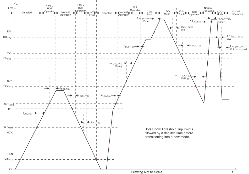
 Figure 7-2 TS Battery Temperature Bias Threshold and Deglitch Timers
 Figure 7-3 Power Up Flow Diagram