JAJSBP7N September 2008 – October 2021 BQ24072 , BQ24073 , BQ24074 , BQ24075 , BQ24079
PRODUCTION DATA
- 1 特長
- 2 アプリケーション
- 3 概要
- 4 Revision History
- 5 概要 (続き)
- 6 Device Comparison Table
- 7 Pin Configuration and Functions
- 8 Specifications
-
9 Detailed Description
- 9.1 Overview
- 9.2 Functional Block Diagram
- 9.3
Feature Description
- 9.3.1 Undervoltage Lockout (UVLO)
- 9.3.2 Power On
- 9.3.3 Overvoltage Protection (OVP)
- 9.3.4 Dynamic Power Path Management
- 9.3.5
Battery Charging
- 9.3.5.1 Charge Current Translator
- 9.3.5.2 Adjustable Termination Threshold (ITERM Input, BQ24074)
- 9.3.5.3 Termination Disable (TD Input, BQ24072, BQ24073)
- 9.3.5.4 Battery Detection and Recharge
- 9.3.5.5 Battery Disconnect (SYSOFF Input, BQ24075, BQ24079)
- 9.3.5.6 Dynamic Charge Timers (TMR Input)
- 9.3.5.7 Status Indicators ( PGOOD, CHG)
- 9.3.5.8 Thermal Regulation and Thermal Shutdown
- 9.3.6 Battery Pack Temperature Monitoring
- 9.4 Device Functional Modes
-
10Application and Implementation
- 10.1 Application Information
- 10.2 Typical Application
- 10.3 System Examples
- 11Power Supply Recommendations
- 12Layout
- 13Device and Documentation Support
- 14Mechanical, Packaging, and Orderable Information
パッケージ・オプション
メカニカル・データ(パッケージ|ピン)
- RGT|16
サーマルパッド・メカニカル・データ
- RGT|16
発注情報
9.3.4.1.1 Input DPM Mode (VIN-DPM)
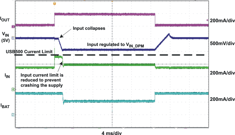
The BQ2407x utilizes the VIN-DPM mode for operation from current-limited USB ports. When EN1 and EN2 are configured for USB100 (EN2=0, EN1=0) or USB500 (EN2=0, EN1=1) modes, the input voltage is monitored. If VIN falls to VIN-DPM, the input current limit is reduced to prevent the input voltage from falling further. This prevents the BQ2407x from crashing poorly designed or incorrectly configured USB sources. Figure 9-3 shows the VIN-DPM behavior to a current limited source. In this figure, the input source has a 400-mA current limit and the device is in USB500 mode (EN1=1, EN2=0).
 Figure 9-3 VIN-DPM Waveform