JAJSL87H january 2010 – april 2021 BQ24090 , BQ24091 , BQ24092 , BQ24093 , BQ24095
PRODUCTION DATA
- 1
- 1 特長
- 2 アプリケーション
- 3 概要
- 4 Revision History
- 5 概要 (続き)
- 6 Device Options
- 7 Pin Configuration and Functions
-
8 Specifications
- 8.1 Absolute Maximum Ratings #GUID-9FC6FB05-10A6-4323-9A52-EE32AE4C5F67/SLUS9405873
- 8.2 ESD Ratings
- 8.3 Recommended Operating Conditions #GUID-4D70561B-CB71-403D-B731-8EF5DEBEBDF9/SLUS9401392
- 8.4 Thermal Information
- 8.5 Dissipation Ratings #GUID-196940BE-C3C2-4CDF-A8A4-7C186292F803/SLUS9404025 #GUID-196940BE-C3C2-4CDF-A8A4-7C186292F803/SLUS9403553
- 8.6 Electrical Characteristics
- 8.7 Typical Characteristics
-
9 Detailed Description
- 9.1 Overview
- 9.2 Functional Block Diagram
- 9.3
Feature Description
- 9.3.1 Power Down or Undervoltage Lockout (UVLO)
- 9.3.2 UVLO
- 9.3.3 Power Up
- 9.3.4 Sleep Mode
- 9.3.5 New Charge Cycle
- 9.3.6 Overvoltage Protection (OVP) – Continuously Monitored
- 9.3.7 Power Good Indication ( PG)
- 9.3.8 CHG Pin Indication
- 9.3.9 CHG and PG LED Pullup Source
- 9.3.10 IN-DPM (VIN-DPM or IN–DPM)
- 9.3.11 OUT
- 9.3.12 ISET
- 9.3.13 PRE_TERM – Precharge and Termination Programmable Threshold
- 9.3.14 ISET2
- 9.3.15 TS
- 9.4 Device Functional Modes
- 10Application and Implementation
- 11Power Supply Recommendations
- 12Layout
- 13Device and Documentation Support
- Mechanical, Packaging, and Orderable Information
パッケージ・オプション
メカニカル・データ(パッケージ|ピン)
- DGQ|10
サーマルパッド・メカニカル・データ
- DGQ|10
発注情報
8.7.2 Protection Circuits Waveforms
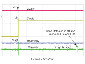
| CH4: Iout (0.2 A/Div) | ||
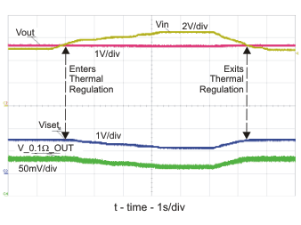
The IC temperature rises to 125°C and enters thermal regulation. Charge current is reduced to regulate the IC at 125°C. VIN is reduced, the IC temperature drops, the charge current returns to the programmed value.
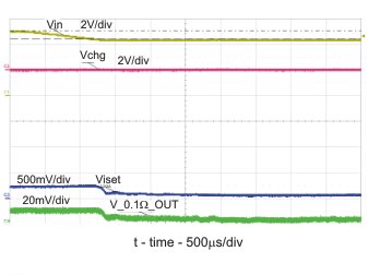
Figure 8-9 Thermal Regulation – Vin increases PWR/Iout Reduced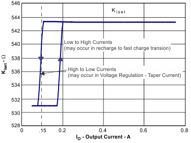 Figure 8-11 KISET for Low and High Currents
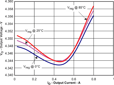 Figure 8-13 Load Regulation –
BQ24095
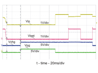
| VIN swept from 5 V to 3.9 V to 5 V | ||
| VBAT = 4 V | ||
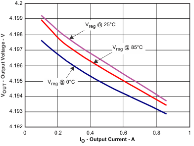 Figure 8-12 Load Regulation
Overtemperature