JAJSOY8H November 2011 – July 2022 BQ24160 , BQ24160A , BQ24161 , BQ24161B , BQ24163 , BQ24168
PRODUCTION DATA
- 1 特長
- 2 アプリケーション
- 3 概要
- 4 Revision History
- 5 Device Comparison Table
- 6 Pin Configuration and Functions
- 7 Specifications
-
8 Detailed Description
- 8.1 Overview
- 8.2 Functional Block Diagram
- 8.3
Feature Description
- 8.3.1 Charge Mode Operation
- 8.3.2 Battery Charging Process
- 8.3.3 Battery Detection
- 8.3.4 Dynamic Power Path Management (DPPM)
- 8.3.5 Input Source Connected
- 8.3.6 Battery Only Connected
- 8.3.7 Battery Discharge FET (BGATE)
- 8.3.8 DEFAULT Mode
- 8.3.9 Safety Timer and Watchdog Timer (BQ24160/BQ24161/BQ24161B/BQ24163 only)
- 8.3.10 D+, D– Based Adapter Detection for the USB Input (D+, D–, BQ24160/0A/3)
- 8.3.11 USB Input Current Limit Selector Input (PSEL, BQ24161/161B/168 only)
- 8.3.12 Hardware Chip Disable Input (CD)
- 8.3.13 LDO Output (DRV)
- 8.3.14 External NTC Monitoring (TS)
- 8.3.15 Thermal Regulation and Protection
- 8.3.16 Input Voltage Protection in Charge Mode
- 8.3.17 Charge Status Outputs (STAT, INT)
- 8.3.18 Good Battery Monitor
- 8.4 Device Functional Modes
- 8.5 Programming
- 8.6
Register Maps
- 8.6.1 Status/Control Register (READ/WRITE)
- 8.6.2 Battery/ Supply Status Register (READ/WRITE)
- 8.6.3 Control Register (READ/WRITE)
- 8.6.4 Control/Battery Voltage Register (READ/WRITE)
- 8.6.5 Vender/Part/Revision Register (READ only)
- 8.6.6 Battery Termination/Fast Charge Current Register (READ/WRITE)
- 8.6.7 VIN-DPM Voltage/ DPPM Status Register
- 8.6.8 Safety Timer/ NTC Monitor Register (READ/WRITE)
- 9 Application and Implementation
- 10Power Supply Recommendations
- 11Layout
- 12Device and Documentation Support
パッケージ・オプション
メカニカル・データ(パッケージ|ピン)
- RGE|24
サーマルパッド・メカニカル・データ
- RGE|24
発注情報
8.3.9 Safety Timer and Watchdog Timer (BQ24160/BQ24161/BQ24161B/BQ24163 only)
At the beginning of charging process, the BQ24160/1/1B/3 starts the safety timer. This timer is active during the entire charging process. If charging has not terminated before the safety timer expires, charging is disabled, the charge parameters are reset to the default values and the CE bit is written to a “1”. The length of the safety timer is selectable using the I2C interface. A single 128-μs pulse is sent on the STAT and INT outputs and the STATx bits of the status registers are updated in the I2C. In DEFAULT mode, the safety timer can be reset and a new charge cycle initiated by input supply power on reset, removing/inserting battery or toggling the CD pin. In HOST mode, the CE bit is set to a '1' when the safety timer expires. The CE bit must be cleared to a '0' in order to resume charging and clear the safety timer fault. The safety timer duration is selectable using the TMR_X bits in the Safety Timer Register/ NTC Monitor register. Changing the safety timer duration resets the safety timer. This function prevents continuous charging of a defective battery. During the fast charge (CC) phase, several events increase the timer duration by 2× if the EN_2X_TMR bit is set in the register.
- The system load current reduces the available charging current.
- The input current needed for the fast charge current is limited by the input current loop.
- The input current is reduced because the VINDPM loop is preventing the supply from crashing.
- The device has entered thermal regulation because the IC junction temperature has exceeded TJ(REG).
- The LOW_CHG bit is set.
- The battery voltage is less than VBATSHORT.
- The battery has entered the JEITA WARM or COLD state via the TS pin
During these events, the timer is slowed by half to extend the timer and prevent any false timer faults. Starting a new charge cycle by VSUPPLY POR or removing/replacing the battery or resuming a charge by toggling the CE or HZ_MODE bits, resets the safety timer. Additionally, thermal shutdown events cause the safety timer to reset.
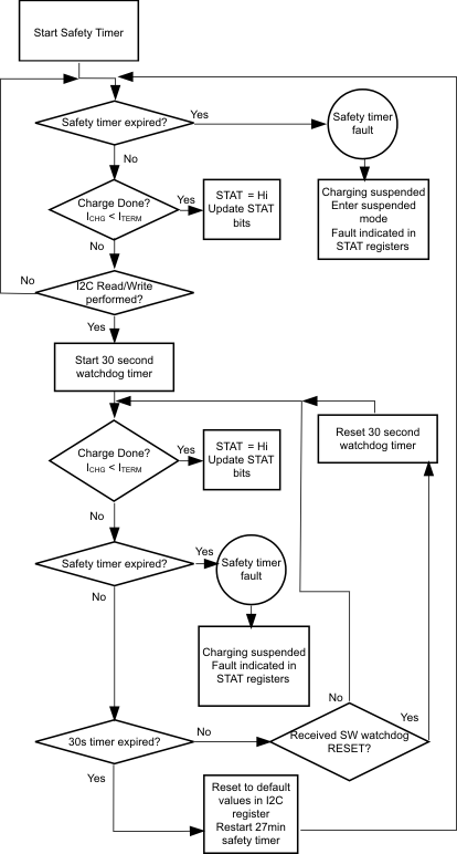
In addition to the safety timer, the BQ24160/1/1B/3 contain a watchdog timer that monitors the host through the I2C interface. Once a read/write is performed on the I2C interface, a 30-second timer (tWATCHDOG) is started. The 30-second timer is reset by the host using the I2C interface. This is done by writing a “1” to the reset bit (TMR_RST) in the control register. The TMR_RST bit is automatically set to “0” when the 30-second timer is reset. This process continues until the battery is fully charged or the safety timer expires. If the 30-second timer expires, the IC enters DEFAULT mode where the default register values are loaded, the safety timer restarts at 27 minutes and charging continues. The I2C may be accessed again to reinitialize the desired values and restart the watchdog timer. The watchdog timer flow chart is shown in Figure 8-3.
 Figure 8-3 The Watchdog Timer Flow
Chart for BQ2416xx