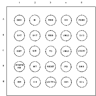
| IN |
A2 |
I |
DC Input Power Supply. IN is connected to the external DC supply. Bypass IN to GND with at least 1 µF of capacitance using a ceramic capacitor. |
| PMID |
A3, B3 |
I/O |
High Side Bypass Connection. Connect at least 3µF of ceramic capacitance with DC bias derating from PMID to GND as close to the PMID and GND pins as possible. |
| GND |
A1, D5 |
| Ground connection. Connect to the ground plane of the circuit. |
| PGND |
A5 |
| Power ground connection. Connect to the ground plane of the circuit. Connect the output filter cap from the buck converter to this ground as shown in the layout example. |
| CD |
E2 |
I |
Chip Disable. Drive CD low to place the part in High-Z mode with battery only present, or enable charging when VIN is valid. Drive CD high for Active Battery mode when battery only is present, and disable charge when VIN is present. CD is pulled low internally with 900 kΩ. |
| SDA |
E4 |
I/O |
I2C Interface Data. Connect SDA to the logic rail through a 10-kΩ resistor. |
| SCL |
E5 |
I |
I2C Interface Clock. Connect SCL to the logic rail through a 10-kΩ resistor. |
| ILIM |
C2 |
I |
Adjustable Input Current Limit Programming. Connect a resistor from ILIM to GND to program the input current limit. The input current includes the system load and the battery charge current. Connect ILIM to GND to set the input current limit to the internal default threshold. ILIM can also be updated through I2C. |
| LSCTRL |
E3 |
I |
Load Switch and LDO Control Input. Pull high to enable the LS/LDO output, pull low to disable the LS/LDO output. |
| ISET |
C1 |
I |
Fast-Charge Current Programming Input. Connect a resistor from ISET to GND to program the fast-charge current level. Connect a resistor from ISET to GND to set the charge current to the internal default. ISET can also be updated through I2C. While charging, the voltage at ISET reflects the actual charging current and can be used to monitor charge current if an ISET resistor is present and the device is not in host mode. |
| IPRETERM |
D1 |
I |
Termination current programming input. Connect a 0-Ω to 10-kΩ resistor from IPRETERM to GND to program the termination current between 5% and 20% of the charge current. The pre-charge current is the same as the termination current setting. Connect IPRETERM to GND to set the termination current to the internal default threshold. IPRETERM can also be updated through I2C. |
| INT |
D2 |
O |
Status Output. INT is an open-drain output that signals charging status and fault interrupts. INT pulls low during charging. INT is high impedance when charging is complete, disabled, or the charger is in high impedance mode. When a fault occurs, a 128µs pulse is sent out as an interrupt for the host. INT charge indicator function is enabled/disabled using the EN_INT bit in the control register. Connect INT to a logic rail using an LED for visual indication of charge status or through a 100kΩ resistor to communicate with the host processor. |
| PG |
D4 |
O |
Open-drain Power Good status indication output. PG pulls to GND when VIN is above V(BAT) + VSLP and less that VOVP. PG is high-impedance when the input power is not within specified limits. Connect PG to the desired logic voltage rail using a 1kΩ to 100kΩ resistor, or use with an LED for visual indication. PG can also be configured as a push-button voltage shifted output (MRS) in the registers, where the output of the PG pin reflects the status of the MR input, but pulled up to the desired logic voltage rail using a 1kΩ to 100kΩ resistor. |
| RESET |
D3 |
O |
Reset Output. RESET is an open drain active low output that goes low when MR is held low for longer than tRESET, which is configurable by the MRRESET registers. RESET is deasserted after the tRESET_D, typically 400ms. |
| MR |
E1 |
I |
Manual Reset Input. MR is a push-button input that must be held low for greater than tRESET to assert the reset output. If MR is pressed for a shorter period, there are two programmable timer events, tWAKE1 and tWAKE2, that trigger an interrupt to the host. The MR input can also be used to bring the device out of Ship mode. |
| SW |
A4 |
O |
Inductor Connection. Connect to the switched side of the external inductor. |
| SYS |
B5 |
I |
System Voltage Sense Connection. Connect SYS to the system output at the output bulk capacitors. Bypass SYS locally with at least 4.7 µF of effective ceramic capacitance. |
| LS/LDO |
C5 |
O |
Load Switch or LDO output. Connect 1 µF of effective ceramic capacitance to this pin to assure stability. Be sure to account for capacitance bias voltage derating when selecting the capacitor. |
| VINLS |
B4, C4 |
I |
Input to the Load Switch / LDO output. Connect 1 µF of effective ceramic capacitance from this pin to GND. |
| BAT |
B1, B2 |
I/O |
Battery Connection. Connect to the positive terminal of the battery. Bypass BAT to GND with at least 1 µF of ceramic capacitance. |
| TS |
C3 |
I |
Battery Pack NTC Monitor. Connect TS to the center tap of a resistor divider from VIN to GND. The NTC is connected from TS to GND. The TS function provides four thresholds for JEITA compatibility. TS faults are reported by the I2C interface during charge mode. |
