JAJSD89C August   2015  – September 2016 BQ25120 , BQ25121

PRODUCTION DATA.  

  1. 特長
  2. アプリケーション
  3. 概要
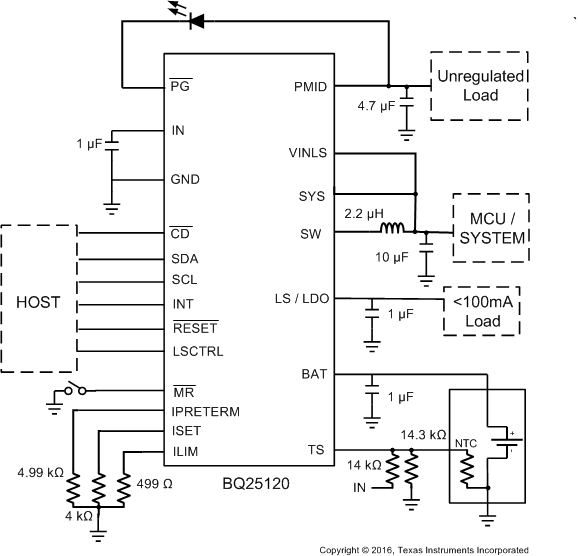
    1.     概略回路図
  4. 改訂履歴
  5. 概要(続き)
  6. Device Comparison Table
  7. Pin Configuration and Functions
    1.     Pin Functions
  8. Specifications
    1. 8.1 Absolute Maximum Ratings
    2. 8.2 ESD Ratings
    3. 8.3 Recommended Operating Conditions
    4. 8.4 Thermal Information
    5. 8.5 Electrical Characteristics
    6. 8.6 Timing Requirements
    7. 8.7 Typical Characteristics
  9. Detailed Description
    1. 9.1 Overview
    2. 9.2 Functional Block Diagram
    3. 9.3 Feature Description
      1. 9.3.1  Ship Mode
      2. 9.3.2  High Impedance Mode
      3. 9.3.3  Active Battery Only Connected
      4. 9.3.4  Voltage Based Battery Monitor
      5. 9.3.5  Sleep Mode
      6. 9.3.6  Input Voltage Based Dynamic Power Management (VIN(DPM))
      7. 9.3.7  Input Overvoltage Protection and Undervoltage Status Indication
      8. 9.3.8  Battery Charging Process and Charge Profile
      9. 9.3.9  Dynamic Power Path Management Mode
      10. 9.3.10 Battery Supplement Mode
      11. 9.3.11 Default Mode
      12. 9.3.12 Termination and Pre-Charge Current Programming by External Components (IPRETERM)
      13. 9.3.13 Input Current Limit Programming by External Components (ILIM)
      14. 9.3.14 Charge Current Programming by External Components (ISET)
      15. 9.3.15 Safety Timer and Watchdog Timer
      16. 9.3.16 External NTC Monitoring (TS)
      17. 9.3.17 Thermal Protection
      18. 9.3.18 Typical Application Power Dissipation
      19. 9.3.19 Status Indicators (PG and INT)
      20. 9.3.20 Chip Disable (CD)
      21. 9.3.21 Buck (PWM) Output
      22. 9.3.22 Load Switch / LDO Output and Control
      23. 9.3.23 Manual Reset Timer and Reset Output (MR and RESET)
    4. 9.4 Device Functional Modes
    5. 9.5 Programming
      1. 9.5.1 Serial Interface Description
      2. 9.5.2 F/S Mode Protocol
    6. 9.6 Register Maps
      1. 9.6.1  Status and Ship Mode Control Register
        1. Table 12. Status and Ship Mode Control Register
      2. 9.6.2  Faults and Faults Mask Register
        1. Table 13. Faults and Faults Mask Register
      3. 9.6.3  TS Control and Faults Masks Register
        1. Table 14. TS Control and Faults Masks Register, Memory Location 0010
      4. 9.6.4  Fast Charge Control Register
        1. Table 15. Fast Charge Control Register
      5. 9.6.5  Termination/Pre-Charge and I2C Address Register
        1. Table 16. Termination/Pre-Charge and I2C Address Register
      6. 9.6.6  Battery Voltage Control Register
        1. Table 17. Battery Voltage Control Register
      7. 9.6.7  SYS VOUT Control Register
        1. Table 18. SYS VOUT Control Register
      8. 9.6.8  Load Switch and LDO Control Register
        1. Table 20. Load Switch and LDO Control Register
      9. 9.6.9  Push-button Control Register
        1. Table 21. Push-button Control Register
      10. 9.6.10 ILIM and Battery UVLO Control Register
        1. Table 22. ILIM and Battery UVLO Control Register, Memory Location 1001
      11. 9.6.11 Voltage Based Battery Monitor Register
        1. Table 23. Voltage Based Battery Monitor Register, Memory Location 1010
      12. 9.6.12 VIN_DPM and Timers Register
        1. Table 24. VIN_DPM and Timers Register
  10. 10Application and Implementation
    1. 10.1 Application Information
    2. 10.2 Typical Application
      1. 10.2.1 Design Requirements
      2. 10.2.2 Detailed Design Procedure
        1. 10.2.2.1 Default Settings
        2. 10.2.2.2 Choose the Correct Inductance and Capacitance
        3. 10.2.2.3 Calculations
          1. 10.2.2.3.1 Program the Fast Charge Current (ISET)
          2. 10.2.2.3.2 Program the Input Current Limit (ILIM)
          3. 10.2.2.3.3 Program the Pre-charge/termination Threshold (IPRETERM)
          4. 10.2.2.3.4 TS Resistors (TS)
      3. 10.2.3 Application Performance Curves
        1. 10.2.3.1 Charger Curves
        2. 10.2.3.2 SYS Output Curves
        3. 10.2.3.3 Load Switch and LDO Curves
        4. 10.2.3.4 LS/LDO Output Curves
        5. 10.2.3.5 Timing Waveforms Curves
  11. 11Power Supply Recommendations
  12. 12Layout
    1. 12.1 Layout Guidelines
    2. 12.2 Layout Example
  13. 13デバイスおよびドキュメントのサポート
    1. 13.1 デバイス・サポート
      1. 13.1.1 デベロッパー・ネットワークの製品に関する免責事項
    2. 13.2 関連リンク
    3. 13.3 ドキュメントの更新通知を受け取る方法
    4. 13.4 コミュニティ・リソース
    5. 13.5 商標
    6. 13.6 静電気放電に関する注意事項
    7. 13.7 Glossary
  14. 14メカニカル、パッケージ、および注文情報

パッケージ・オプション

メカニカル・データ(パッケージ|ピン)
サーマルパッド・メカニカル・データ
発注情報

Typical Application

BQ25120 BQ25121 Typ_App_Schematic_slusbz9.gifFigure 35. Typical Application Circuit