JAJSQV7 july   2023 BQ25173-Q1

PRODUCTION DATA  

  1.   1
  2. 特長
  3. アプリケーション
  4. 概要
  5. Revision History
  6. Pin Configuration and Functions
  7. Specifications
    1. 6.1 Absolute Maximum Ratings
    2. 6.2 ESD Ratings
    3. 6.3 Recommended Operating Conditions
    4. 6.4 Thermal Information
    5. 6.5 Electrical Characteristics
    6. 6.6 Timing Requirements
    7. 6.7 Typical Characteristics
  8. Detailed Description
    1. 7.1 Overview
    2. 7.2 Functional Block Diagram
    3. 7.3 Feature Description
      1. 7.3.1 Device Power Up from Input Source
        1. 7.3.1.1 ISET Pin Detection
      2. 7.3.2 Supercapacitor Regulation Voltage
      3. 7.3.3 Supercapacitor Charging Profile
      4. 7.3.4 Status Outputs (PG, STAT)
        1. 7.3.4.1 Power Good Indicator (PG Pin)
        2. 7.3.4.2 Charging Status Indicator (STAT)
      5. 7.3.5 Protection Features
        1. 7.3.5.1 Input Overvoltage Protection (VIN OVP)
        2. 7.3.5.2 Output Overcurrent Protection (OUT OCP)
        3. 7.3.5.3 Thermal Regulation and Thermal Shutdown (TREG and TSHUT)
    4. 7.4 Device Functional Modes
      1. 7.4.1 Shutdown or Undervoltage Lockout (UVLO)
      2. 7.4.2 Sleep Mode
      3. 7.4.3 Active Mode
        1. 7.4.3.1 Standby Mode
      4. 7.4.4 Fault Mode
  9. Application and Implementation
    1. 8.1 Application Information
    2. 8.2 Typical Applications
      1. 8.2.1 1s Supercapacitor Charger Design Example
        1. 8.2.1.1 Design Requirements
        2. 8.2.1.2 Detailed Design Procedure
        3. 8.2.1.3 Application Curves
      2. 8.2.2 4s Supercapacitor Charger Design Example
        1. 8.2.2.1 Design Requirements
        2. 8.2.2.2 Application Curves
  10. Power Supply Recommendations
  11. 10Layout
    1. 10.1 Layout Guidelines
    2. 10.2 Layout Example
    3. 10.3 Thermal Considerations
  12. 11Device and Documentation Support
    1. 11.1 Device Support
      1. 11.1.1 サード・パーティ製品に関する免責事項
    2. 11.2 ドキュメントの更新通知を受け取る方法
    3. 11.3 サポート・リソース
    4. 11.4 Trademarks
    5. 11.5 静電気放電に関する注意事項
    6. 11.6 用語集
  13. 12Mechanical, Packaging, and Orderable Information

パッケージ・オプション

メカニカル・データ(パッケージ|ピン)
サーマルパッド・メカニカル・データ
発注情報

Application Curves

CIN = 1 µF, COUT = 1 µF, CSC = 25 F, VIN = 5 V (unless otherwise specified)
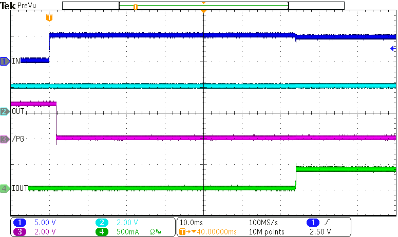
GUID-2FC74FF2-BA27-4B91-B736-D8EB3F49F79D-low.png

ICHG = 400 mA

Figure 8-2 Power Up with Supercapacitor
GUID-649E43EF-D6CB-41B2-B983-EA1C792D9140-low.png
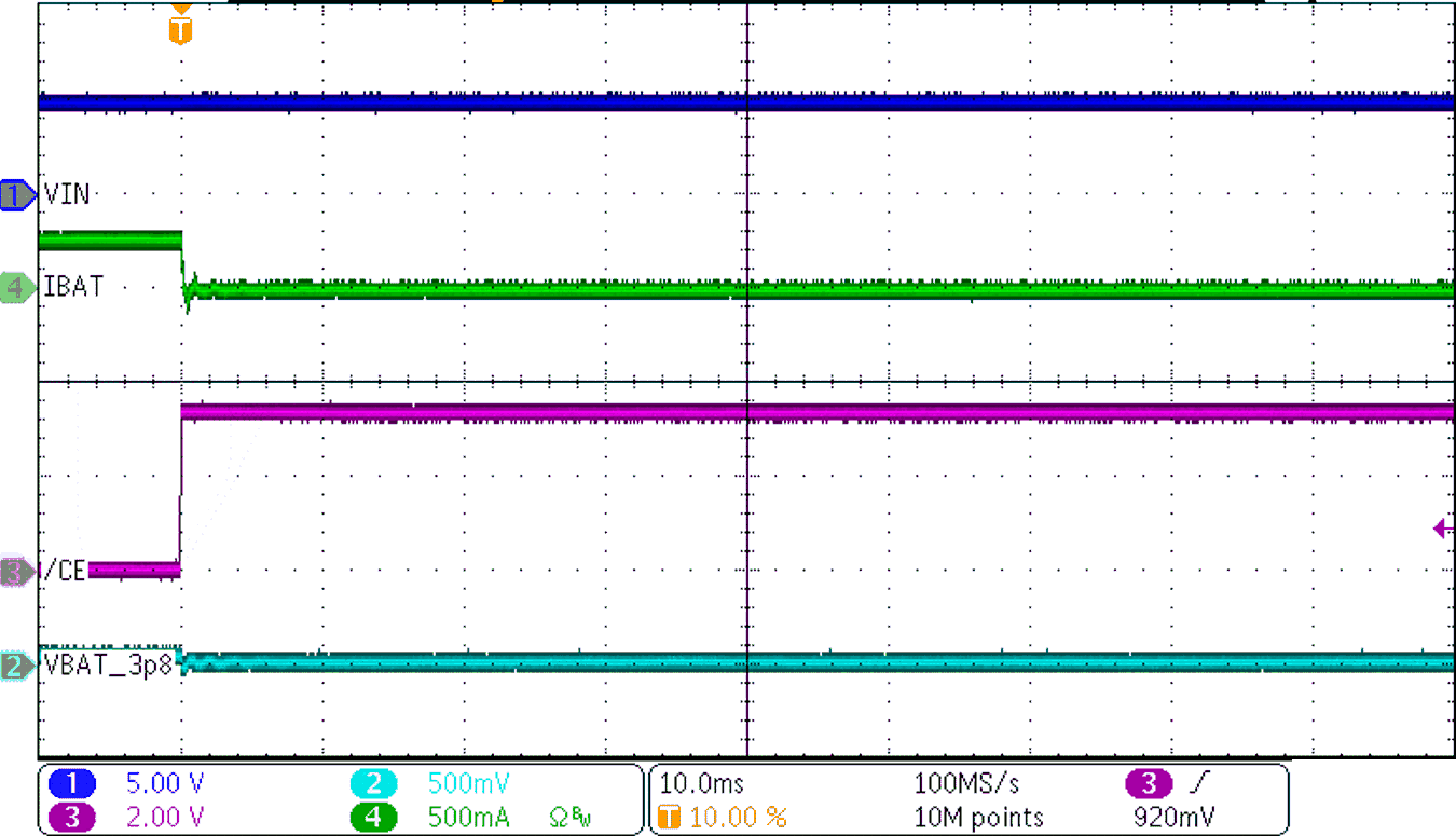
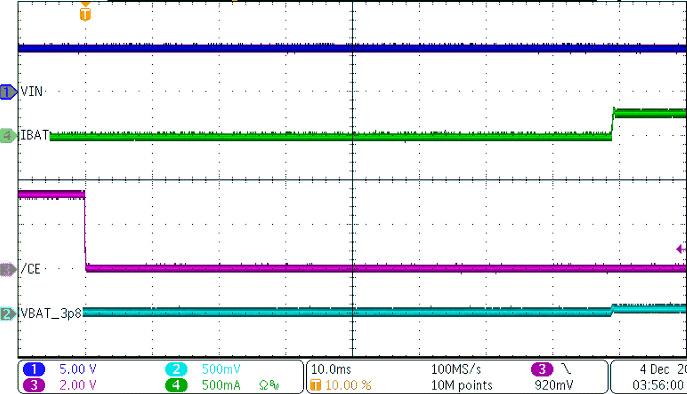
/CE pulled highICHG = 250 mA
Figure 8-4 Charge Disable
GUID-BEB72DD8-212A-4E95-AC56-447F7AAF75CC-low.png
VIN = 5 V → 20 VICHG = 400 mA
Figure 8-6 IN OVP Response
GUID-D0A140F5-67B7-45B2-AB27-C8C49C39543C-low.png
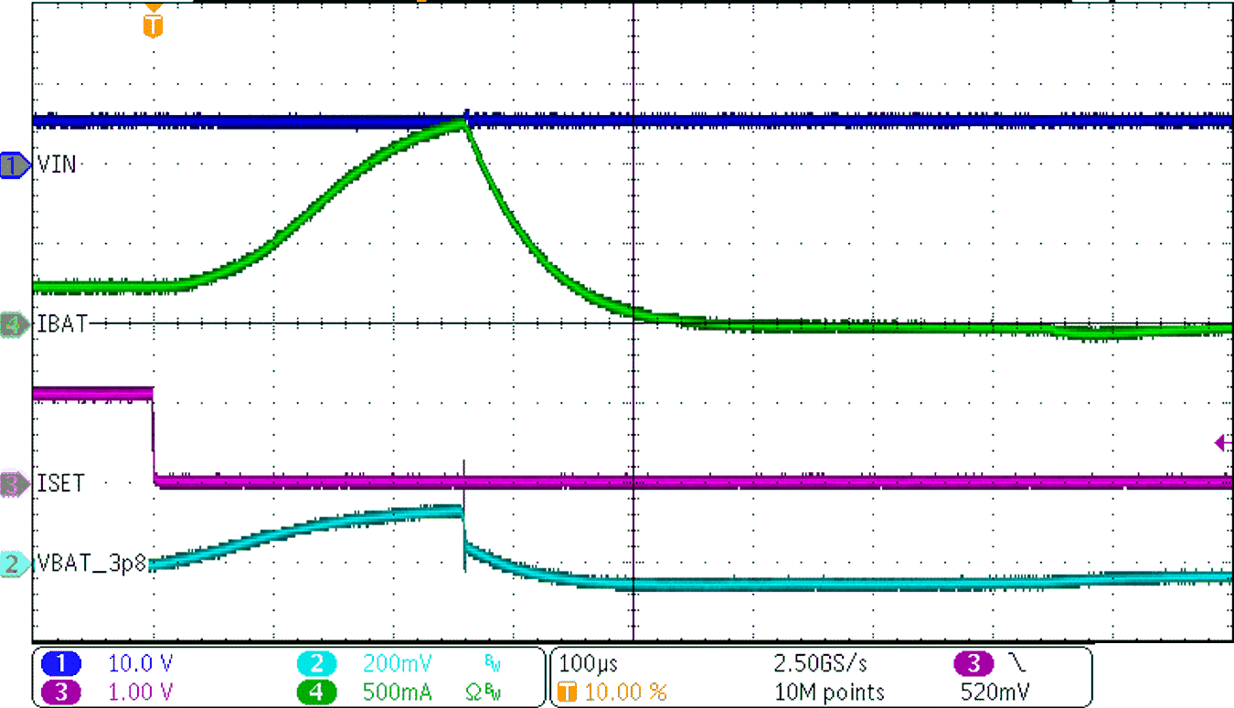
ISET = 1.2 kΩ → 0 Ω
Figure 8-8 ISET Short-Circuit Response
GUID-F24E5F14-5A27-4678-9C00-5CCA7750C0C8-low.png
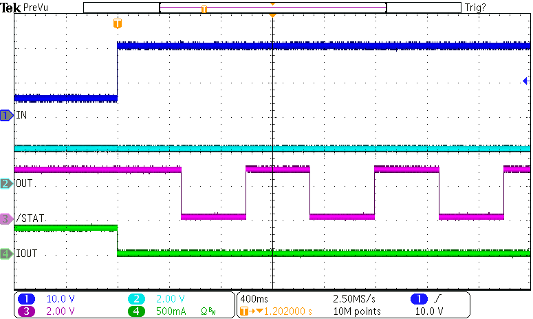
VREG = 2.5 VICHG = 400 mA
Figure 8-10 Charge Complete
GUID-88EA6182-8CAB-4440-BF9C-E29AE792B6B9-low.png
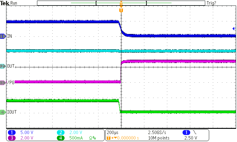
ICHG = 400 mA
Figure 8-3 Power Down with Supercapacitor
GUID-77FE3468-F588-4EB3-A2F5-225F0810107B-low.png
/CE pulled lowICHG = 400 mA
Figure 8-5 Charge Enable
GUID-33A7F553-6D08-4EAB-AC93-6043E367FB0A-low.png
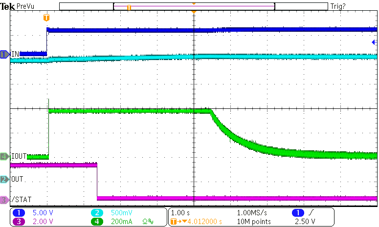
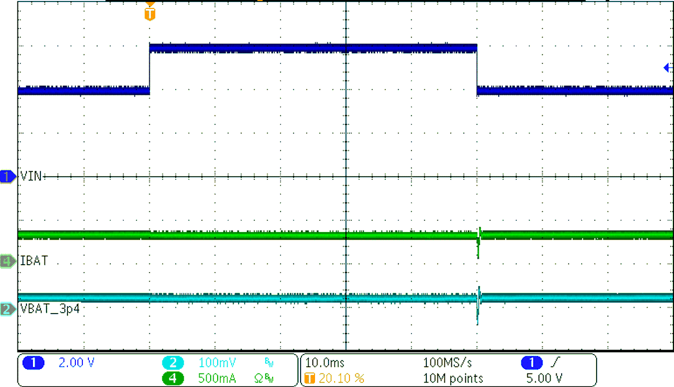
VIN = 4 V → 6 VVOUT = 3.5 V

ICHG = 250 mA

Figure 8-7 IN Transient Response
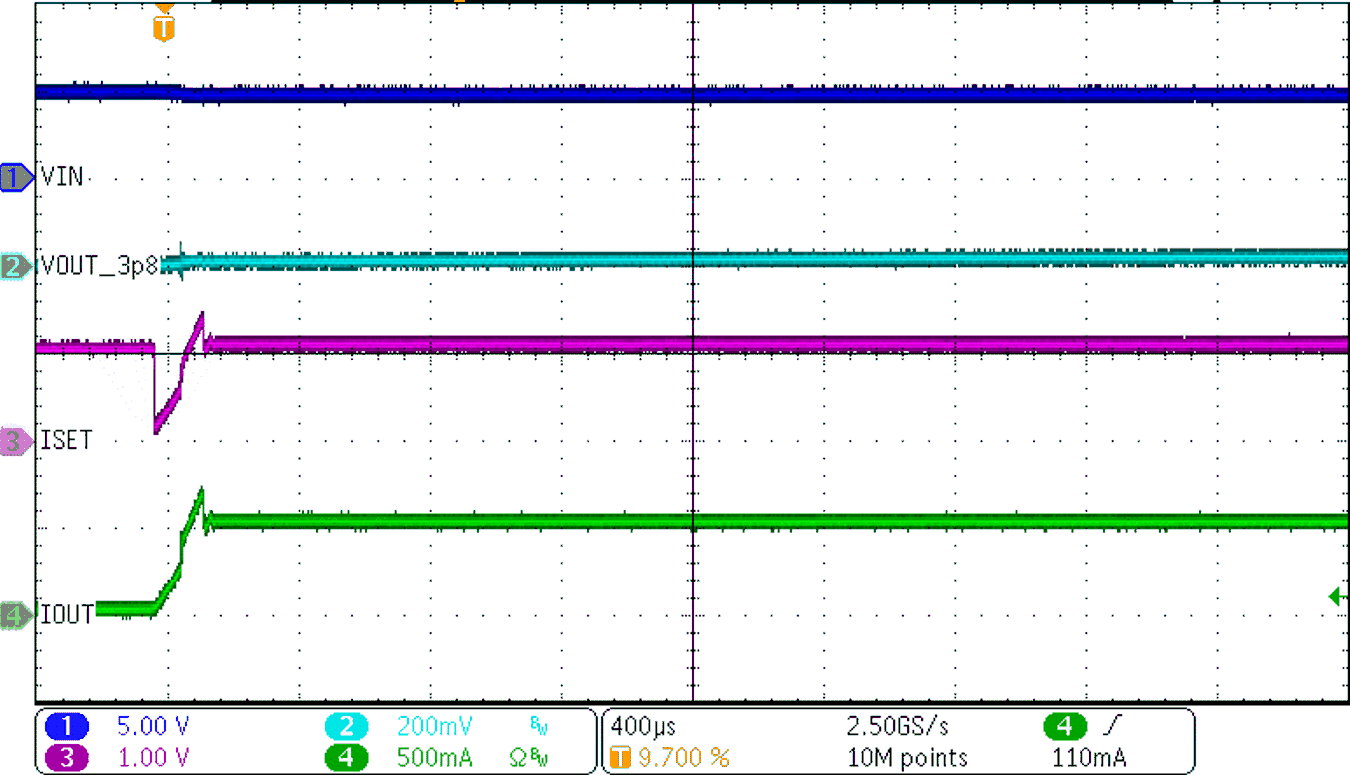
GUID-025C8A39-84A7-4B04-A03C-1BB8175776EE-low.png
ISET = 50 mA → 500 mA
Figure 8-9 ISET Change Response