JAJSQV7 july 2023 BQ25173-Q1
PRODUCTION DATA
- 1
- 1 特長
- 2 アプリケーション
- 3 概要
- 4 Revision History
- 5 Pin Configuration and Functions
- 6 Specifications
- 7 Detailed Description
- 8 Application and Implementation
- 9 Power Supply Recommendations
- 10Layout
- 11Device and Documentation Support
- 12Mechanical, Packaging, and Orderable Information
7.1 Overview
The BQ25173-Q1 is an automotive rated, 800-mA linear charger for 1- to 4-cell supercapacitors targeted at space-limited applications. The device has a single power output that charges the supercapacitor. The system load can be placed in parallel with the supercapacitor and the charge current is shared between the system and supercapacitor.
The charger is designed for a single path from the input to the output to charge the supercapacitor. Upon application of a valid input power source, the ISET pin is checked for short circuit.
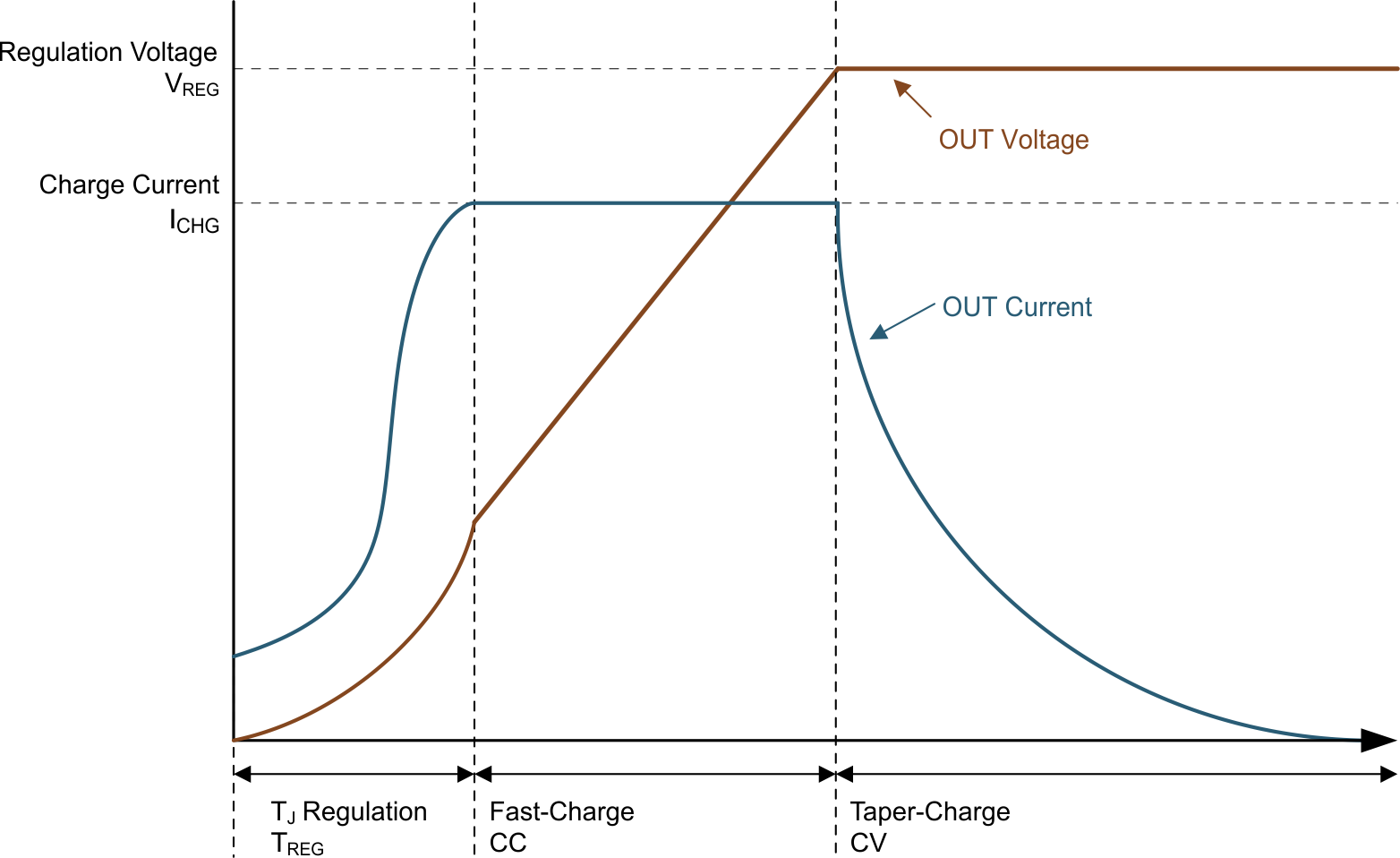
The device attempts to charge the supercapacitor at the fast-charge current setting from fully discharged (0 V) up to the programmable regulation voltage, VREG. Power dissipation in the IC is greatest in fast charge with a lower supercapacitor voltage. If the IC temperature reaches TREG, the IC enters thermal regulation and reduces the charge current as needed to keep the temperature from rising any further. The fast-charge current is programmed using the ISET pin. Figure 7-1 shows the typical supercapacitor charging profile with thermal regulation. At lower fast-charge settings, the junction temperature of the IC is less than TREG and thermal regulation is not entered.
Once the supercapacitor has charged to the regulation voltage, the voltage loop takes control and holds the voltage at the regulation voltage as the current tapers down to zero. There is no current termination threshold as seen in Li-ion chargers.
Further details are described in Section 7.3.
 Figure 7-1 Supercapacitor Charging Profile with Thermal Regulation