JAJSQV7 july   2023 BQ25173-Q1

PRODUCTION DATA  

  1.   1
  2. 特長
  3. アプリケーション
  4. 概要
  5. Revision History
  6. Pin Configuration and Functions
  7. Specifications
    1. 6.1 Absolute Maximum Ratings
    2. 6.2 ESD Ratings
    3. 6.3 Recommended Operating Conditions
    4. 6.4 Thermal Information
    5. 6.5 Electrical Characteristics
    6. 6.6 Timing Requirements
    7. 6.7 Typical Characteristics
  8. Detailed Description
    1. 7.1 Overview
    2. 7.2 Functional Block Diagram
    3. 7.3 Feature Description
      1. 7.3.1 Device Power Up from Input Source
        1. 7.3.1.1 ISET Pin Detection
      2. 7.3.2 Supercapacitor Regulation Voltage
      3. 7.3.3 Supercapacitor Charging Profile
      4. 7.3.4 Status Outputs (PG, STAT)
        1. 7.3.4.1 Power Good Indicator (PG Pin)
        2. 7.3.4.2 Charging Status Indicator (STAT)
      5. 7.3.5 Protection Features
        1. 7.3.5.1 Input Overvoltage Protection (VIN OVP)
        2. 7.3.5.2 Output Overcurrent Protection (OUT OCP)
        3. 7.3.5.3 Thermal Regulation and Thermal Shutdown (TREG and TSHUT)
    4. 7.4 Device Functional Modes
      1. 7.4.1 Shutdown or Undervoltage Lockout (UVLO)
      2. 7.4.2 Sleep Mode
      3. 7.4.3 Active Mode
        1. 7.4.3.1 Standby Mode
      4. 7.4.4 Fault Mode
  9. Application and Implementation
    1. 8.1 Application Information
    2. 8.2 Typical Applications
      1. 8.2.1 1s Supercapacitor Charger Design Example
        1. 8.2.1.1 Design Requirements
        2. 8.2.1.2 Detailed Design Procedure
        3. 8.2.1.3 Application Curves
      2. 8.2.2 4s Supercapacitor Charger Design Example
        1. 8.2.2.1 Design Requirements
        2. 8.2.2.2 Application Curves
  10. Power Supply Recommendations
  11. 10Layout
    1. 10.1 Layout Guidelines
    2. 10.2 Layout Example
    3. 10.3 Thermal Considerations
  12. 11Device and Documentation Support
    1. 11.1 Device Support
      1. 11.1.1 サード・パーティ製品に関する免責事項
    2. 11.2 ドキュメントの更新通知を受け取る方法
    3. 11.3 サポート・リソース
    4. 11.4 Trademarks
    5. 11.5 静電気放電に関する注意事項
    6. 11.6 用語集
  13. 12Mechanical, Packaging, and Orderable Information

パッケージ・オプション

メカニカル・データ(パッケージ|ピン)
サーマルパッド・メカニカル・データ
発注情報

Supercapacitor Regulation Voltage

The device allows for the supercapacitor regulation voltage, VREG, to be programmed with a resistor divider between the OUT and FB pins:

Equation 2. VREG= VFB_REF×RFBT+RFBBRFBB

Where VFB_REF is listed in the electrical characteristcs table. The resistors can be seen in Figure 7-2. The total resistance (RFBT + RFBB) should not exceed 1 MΩ.
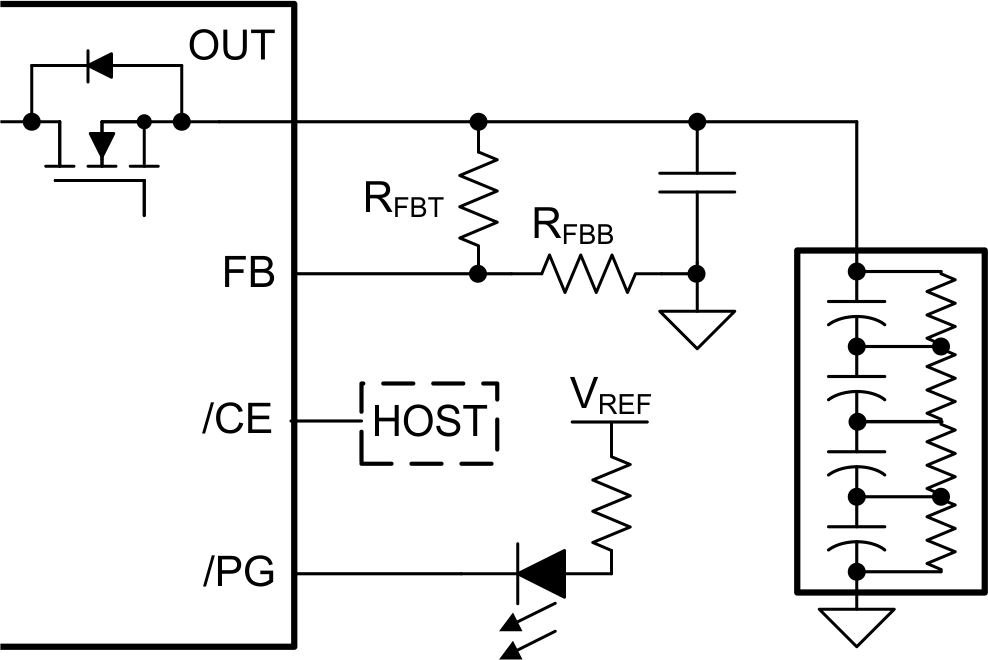
GUID-FE6E683E-3925-4873-B6F4-3028D0950C70-low.pngFigure 7-2 BQ25173-Q1 Feedback Divider