JAJSKR2 February   2021 BQ25303J

PRODUCTION DATA  

  1.   1
  2. 特長
  3. アプリケーション
  4. 概要
  5. Revision History
  6. 概要 (続き)
  7. Device Comparison Table
  8. Pin Configuration and Functions
  9. Specifications
    1. 8.1 Absolute Maximum Ratings
    2. 8.2 ESD Ratings
    3. 8.3 Recommended Operating Conditions
    4. 8.4 Thermal Information
    5. 8.5 Electrical Characteristics
    6. 8.6 Timing Requirements
    7. 8.7 Typical Characteristics
  10. Detailed Description
    1. 9.1 Overview
    2. 9.2 Functional Block Diagram
    3. 9.3 Feature Description
      1. 9.3.1 Device Power Up
        1. 9.3.1.1 Power-On-Reset (POR)
        2. 9.3.1.2 REGN Regulator Power Up
        3. 9.3.1.3 Charger Power Up
        4. 9.3.1.4 Charger Enable and Disable by EN Pin
        5. 9.3.1.5 Device Unplugged from Input Source
      2. 9.3.2 Battery Charging Management
        1. 9.3.2.1 Battery Charging Profile
        2. 9.3.2.2 Precharge
        3. 9.3.2.3 Charging Termination
        4. 9.3.2.4 Battery Recharge
        5. 9.3.2.5 Charging Safety Timer
        6. 9.3.2.6 Thermistor Temperature Monitoring
      3. 9.3.3 Charging Status Indicator (STAT)
      4. 9.3.4 Protections
        1. 9.3.4.1 Voltage and Current Monitoring
          1. 9.3.4.1.1 Input Over-Voltage Protection
          2. 9.3.4.1.2 Input Voltage Dynamic Power Management (VINDPM)
          3. 9.3.4.1.3 Input Current Limit
          4. 9.3.4.1.4 Cycle-by-Cycle Current Limit
        2. 9.3.4.2 Thermal Regulation and Thermal Shutdown
        3. 9.3.4.3 Battery Protection
          1. 9.3.4.3.1 Battery Over-Voltage Protection (VBAT_OVP)
          2. 9.3.4.3.2 Battery Short Circuit Protection
        4. 9.3.4.4 ICHG Pin Open and Short Protection
    4. 9.4 Device Functional Modes
      1. 9.4.1 Disable Mode, HiZ Mode, Sleep Mode, Charge Mode, Termination Mode, and Fault Mode
  11. 10Application and Implementation
    1. 10.1 Application Information
    2. 10.2 Typical Applications
      1. 10.2.1 Typical Application
        1. 10.2.1.1 Design Requirements
        2. 10.2.1.2 Detailed Design Procedure
          1. 10.2.1.2.1 Charge Voltage Settings
          2. 10.2.1.2.2 Charge Current Setting
          3. 10.2.1.2.3 Inductor Selection
          4. 10.2.1.2.4 Input Capacitor
          5. 10.2.1.2.5 Output Capacitor
        3. 10.2.1.3 Application Curves
      2. 10.2.2 Typical Application with External Power Path
        1. 10.2.2.1 Design Requirements
        2. 10.2.2.2 Detailed Design Procedure
        3. 10.2.2.3 Application Curves
  12. 11Power Supply Recommendations
  13. 12Layout
    1. 12.1 Layout Guidelines
    2. 12.2 Layout Example
  14. 13Device and Documentation Support
    1. 13.1 Device Support
      1. 13.1.1 サード・パーティ製品に関する免責事項
    2. 13.2 ドキュメントの更新通知を受け取る方法
    3. 13.3 サポート・リソース
    4. 13.4 Trademarks
    5. 13.5 静電気放電に関する注意事項
    6. 13.6 用語集
  15. 14Mechanical, Packaging, and Orderable Information

パッケージ・オプション

メカニカル・データ(パッケージ|ピン)
サーマルパッド・メカニカル・データ
発注情報

Thermistor Temperature Monitoring

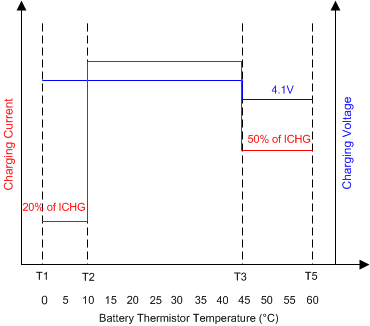
The charger device provides a single thermistor input TS pin for battery temperature monitor. To improve the safety of charging Li-ion batteries, JEITA guideline was released on April 20, 2007. The guideline emphasized the importance of avoiding a high charge current and high charge voltage at certain low and high temperature ranges. To initiate a charge cycle, the voltage on TS pin must be within the VT1% to VT5% thresholds. If TS voltage is out of T1-T5 temperature range, the charger stops charging and waits until the battery temperature is within the T1 to T5 range. .

At cool temperature (T1-T2), the charge current is reduced to 20% of the set fast charge if RICHG < RICHG_HIGH. If RICHG > RICHG_HIGH, the charge current is reduced to 50% of fast charge current in cool charge. At normal temperature (T2 - T3), the charger charges battery as fast charge and the fast charge current is set by a resister at ICHG pin. At warm temperature (T3 -T5), the charge voltage is reduced to 4.1 V and 50% of fast charge current. If the charge voltage is set below 4.1V, the charge voltage will remain unchanged during warm charge.

RT1 and RT2 programs temperatures from T1 to T5. In the equations, RNTC,T1 is NTC thermistor resistance value at temperature T1 and RNTC,T5 is NTC thermistor resistance values at temperature T5. Select 0°C to 60°C for battery charge temperature range, then NTC thermistor 103AT-2 thermistor resistance is RNTC,T1 = 27.28 kΩ ( at 0°C) and RNTC,T5 = 3.02 kΩ (at 60°C), from the Equation 1 and Equation 2, RT1 and RT2 are derived as:

• RT1 = 4.32 kΩ

• RT1 = 21 kΩ
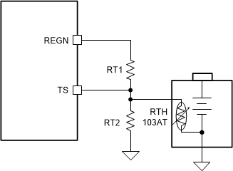
BQ25303J Battery Temperature Sensing
                    Circuit Figure 9-2 Battery Temperature Sensing Circuit
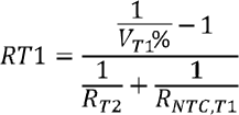
Equation 1. BQ25303J
Equation 2. BQ25303J
Equation 3.
Equation 4.
BQ25303J JEITA ProfileFigure 9-3 JEITA Profile