JAJSGP9G October   2011  – August 2023 BQ25504

PRODUCTION DATA  

  1.   1
  2. 特長
  3. アプリケーション
  4. 概要
  5. Revision History
  6. 概要 (続き)
  7. Pin Configuration and Functions
  8. Specifications
    1. 7.1 Absolute Maximum Ratings
    2. 7.2 ESD Ratings
    3. 7.3 Recommended Operating Conditions
    4. 7.4 Thermal Information
    5. 7.5 Electrical Characteristics
    6. 7.6 Typical Characteristics
  9. Detailed Description
    1. 8.1 Overview
    2. 8.2 Functional Block Diagram
    3. 8.3 Feature Description
      1. 8.3.1 Maximum Power Point Tracking
      2. 8.3.2 Battery Undervoltage Protection
      3. 8.3.3 Battery Overvoltage Protection
      4. 8.3.4 Battery Voltage in Operating Range (VBAT_OK Output)
      5. 8.3.5 Nano-Power Management and Efficiency
    4. 8.4 Device Functional Modes
      1. 8.4.1 Cold-Start Operation (VSTOR < VSTOR_CHGEN, VIN_DC > VIN(CS) and PIN > PIN(CS))
      2. 8.4.2 Main Boost Charger Enabled (VSTOR > VSTOR_CHGEN, VIN_DC > VIN(DC) and EN = LOW )
      3. 8.4.3 Thermal Shutdown
  10. Application and Implementation
    1. 9.1 Application Information
      1. 9.1.1 Storage Element Selection
      2. 9.1.2 Inductor Selection
      3. 9.1.3 Capacitor Selection
        1. 9.1.3.1 VREF_SAMP Capacitance
        2. 9.1.3.2 VIN_DC Capacitance
        3. 9.1.3.3 VSTOR Capacitance
        4. 9.1.3.4 Additional Capacitance on VSTOR or VBAT
    2. 9.2 Typical Applications
      1. 9.2.1 Solar Application Circuit
        1. 9.2.1.1 Design Requirements
        2. 9.2.1.2 Detailed Design Procedure
        3. 9.2.1.3 Application Curves
      2. 9.2.2 TEG Application Circuit
        1. 9.2.2.1 Design Requirements
        2. 9.2.2.2 Detailed Design Procedure
        3. 9.2.2.3 Application Curves
      3. 9.2.3 MPPT Disabled, Low Impedance Source Application Circuit
        1. 9.2.3.1 Design Requirements
        2. 9.2.3.2 Detailed Design Procedure
        3. 9.2.3.3 Application Curves
  11. 10Power Supply Recommendations
  12. 11Layout
    1. 11.1 Layout Guidelines
    2. 11.2 Layout Example
    3. 11.3 Thermal Considerations
  13. 12Device and Documentation Support
    1. 12.1 Device Support
      1. 12.1.1 サード・パーティ製品に関する免責事項
      2. 12.1.2 Zip Files
    2. 12.2 Documentation Support
      1. 12.2.1 Related Documentation
    3. 12.3 ドキュメントの更新通知を受け取る方法
    4. 12.4 サポート・リソース
    5. 12.5 Trademarks
    6. 12.6 静電気放電に関する注意事項
    7. 12.7 用語集
  14. 13Mechanical, Packaging, and Orderable Information

パッケージ・オプション

メカニカル・データ(パッケージ|ピン)
サーマルパッド・メカニカル・データ
発注情報

Additional Capacitance on VSTOR or VBAT

If there are large, fast system load transients and/or the storage element has high resistance, then the CSTOR capacitors may momentarily discharge below the VBAT_UV threshold in response to the transient. This causes the BQ25504 to turn off the PFET switch between VSTOR and VBAT and turn on the boost charger. The CSTOR capacitors may further discharge below the VSTOR_CHGEN threshold and cause the BQ25504 to enter Cold Start. For instance, some Li-ion batteries or thin-film batteries may not have the current capacity to meet the surge current requirements of an attached low power radio. To prevent VSTOR from drooping, either increasing the CSTOR capacitance or adding additional capacitance in parallel with the storage element is recommended. For example, if boost charger is configured to charge the storage element to 4.2 V and a 500 mA load transient of 50 µs duration infrequently occurs, then, solving I = C x dv/dt for CSTOR gives:

Equation 9. GUID-4DAFD8D2-2CA8-42DD-8E04-A2EBF59C5729-low.gif

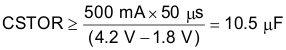
Note that increasing CSTOR is the recommended solution but will cause the boost charger to operate in the less efficient cold start mode for a longer period at startup compared to using CSTOR = 4.7 µF. If longer cold start run times are not acceptable, then place the additional capacitance in parallel with the storage element.

For a recommended list of standard components, see the EVM User’s Guide (SLUUAA8).