JAJSGP9G October 2011 – August 2023 BQ25504
PRODUCTION DATA
- 1
- 1 特長
- 2 アプリケーション
- 3 概要
- 4 Revision History
- 5 概要 (続き)
- 6 Pin Configuration and Functions
- 7 Specifications
- 8 Detailed Description
- 9 Application and Implementation
- 10Power Supply Recommendations
- 11Layout
- 12Device and Documentation Support
- 13Mechanical, Packaging, and Orderable Information
パッケージ・オプション
メカニカル・データ(パッケージ|ピン)
- RGT|16
サーマルパッド・メカニカル・データ
- RGT|16
発注情報
8.4.2 Main Boost Charger Enabled (VSTOR > VSTOR_CHGEN, VIN_DC > VIN(DC) and EN = LOW )
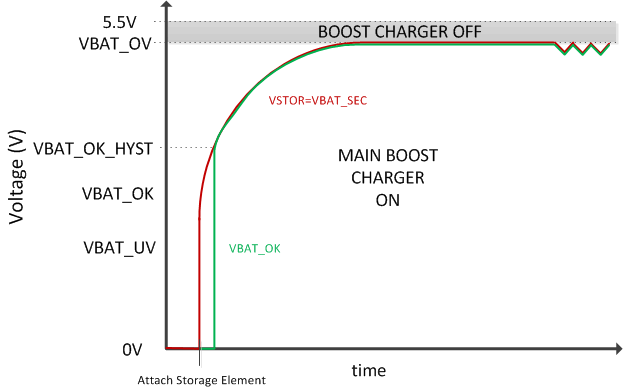
One way to avoid cold start is to attach a partially charged storage element as shown in Figure 8-3.
 Figure 8-3 Charger Operation after a Partially Charged Storage Element is Attached and Harvester Power is Available
When no input source is attached, the VSTOR node should be discharged to ground before attaching a storage element. Hot-plugging a storage element that is charged (e.g., the battery protector PFET is closed) and with the VSTOR node more than 100 mV above ground results in the PFET between VSTOR and VBAT remaining off until an input source is attached.
Assuming the voltages on VSTOR and VBAT are both below 100mV, when a charged storage element is attached (i.e. hot-plugged) to VBAT, the IC.
- first turns on the internal PFET between the VSTOR and VBAT pins for tBAT_HOT_PLUG (45ms) in order to charge VSTOR to VSTOR_CHGEN then turns off the PFET to prevent the battery from overdischarge,
- then performs an initialization pulse on VRDIV to reset the feedback voltages,
- then disables the charger for 32 ms (typical) to allow the VIN_DC voltage to rise to the harvester's open-circuit voltage which will be used as the input voltage regulation reference voltage until the next MPPT sampling cycle and
- lastly performs its first feedback sampling using VRDIV, approximately 64 ms after the initialization pulse.
If the VSTOR pin voltage remains above the internal under voltage threshold (VBAT_UV) for the additional 64 ms after the VRDIV initialization pulse (following the 45-ms PFET on time), the internal PFET turns back on and the main boost charger begins to charge the storage element assuming there is sufficient power available from the harvester at the VIN_DC pin. If VSTOR does not reach the VBAT_UV threshold, then the PFET remains off until the main boost charger can raise the VSTOR voltage to VBAT_UV. If a system load tied to VSTOR discharges VSTOR below VSTOR_GEN or below VBAT_UV during the 32 ms initial MPPT reference voltage measurement or within 110 ms after hot plug, it is recommended to add an external PFET between the system load and VSTOR. An inverted VBAT_OK signal can be used to drive the gate of this system-isolating, external PFET. Otherwise, the VSTOR voltage waveform will have incremental pulses as the IC turns on and off the internal PFET controlled by VBAT_UV or cycles between cold-start and main boost charger operation.
Once VSTOR is above VSTOR_CHGEN, the main boost charger employs pulse frequency modulation (PFM) mode of control to regulate the voltage at VIN_DC close to the desired reference voltage. The reference voltage is set by the MPPT control scheme as described in the features section. Input voltage regulation is obtained by transferring charge from the input to VSTOR only when the input voltage is higher than the voltage on pin VREF_SAMP. The current through the inductor is controlled through internal current sense circuitry. The peak current in the inductor is dithered internally to up to three pre-determined levels in order to maintain high efficiency of the charger across a wide input current range. The charger transfers up to a maximum of 100 mA average input current (230mA typical peak inductor current). The boost charger is disabled when the voltage on VSTOR reaches the user set VBAT_OV threshold to protect the battery connected at VBAT from overcharging. In order for the battery to charge to VBAT_OV, the input power must exceed the power needed for the load on VSTOR. See the Section 10 section for guidance on minimum input power requirements.
Steady state operation for the boost charger is shown in Figure 9-3. These plots highlight the inductor current, the VSTOR voltage ripple, input voltage regulation and the LBOOST switching node. The cycle-by-cycle minor switching frequency is a function of the boost converter's inductor value, peak current limit and voltage levels on each side of each inductor. Once the VSTOR capacitor, CSTOR, droops below a minimum value, the hysteretic switching repeats.
If VIN_DC is higher than VSTOR and VSTOR is higher than VBAT_OV, the input VIN_DC is pulled to ground through a small resistance to stop further charging of the attached battery or capacitor. It is critical that if this case is expected, the impedance of the source attached to VIN_DC be higher than 20 Ω and not a low impedance source.