SLUSEC9B October   2020  – July 2024 BQ25618E , BQ25619E

PRODUCTION DATA  

  1.   1
  2. Features
  3. Applications
  4. Description
  5. Description (continued)
  6. Device Comparison Table
  7. Pin Configuration and Functions
  8. Specifications
    1. 7.1 Absolute Maximum Ratings
    2. 7.2 ESD Ratings
    3. 7.3 Recommended Operating Conditions
    4. 7.4 Thermal Information
    5. 7.5 Electrical Characteristics
    6. 7.6 Timing Requirements
    7. 7.7 Typical Characteristics
  9. Detailed Description
    1. 8.1 Overview
    2. 8.2 Functional Block Diagram
    3. 8.3 Feature Description
      1. 8.3.1 Power-On-Reset (POR)
      2. 8.3.2 Device Power Up From Battery Without Input Source
      3. 8.3.3 Power Up From Input Source
        1. 8.3.3.1 Power Up REGN LDO
        2. 8.3.3.2 Poor Source Qualification
        3. 8.3.3.3 Input Source Type Detection (IINDPM Threshold)
          1. 8.3.3.3.1 PSEL Pins Sets Input Current Limit
        4. 8.3.3.4 Input Voltage Limit Threshold Setting (VINDPM Threshold)
        5. 8.3.3.5 Power Up Converter in Buck Mode
        6. 8.3.3.6 HIZ Mode with Adapter Present
      4. 8.3.4 Power Path Management
        1. 8.3.4.1 Narrow Voltage DC (NVDC) Architecture
        2. 8.3.4.2 Dynamic Power Management
        3. 8.3.4.3 Supplement Mode
      5. 8.3.5 Battery Charging Management
        1. 8.3.5.1 Autonomous Charging Cycle
        2. 8.3.5.2 Battery Charging Profile
        3. 8.3.5.3 Charging Termination
        4. 8.3.5.4 Thermistor Qualification
          1. 8.3.5.4.1 JEITA Guideline Compliance During Charging Mode
        5. 8.3.5.5 Charging Safety Timer
      6. 8.3.6 Ship Mode and QON Pin
        1. 8.3.6.1 BATFET Disable (Enter Ship Mode)
        2. 8.3.6.2 BATFET Enable (Exit Ship Mode)
        3. 8.3.6.3 BATFET Full System Reset
      7. 8.3.7 Status Outputs ( STAT, INT , PG )
        1. 8.3.7.1 Power Good Indicator (PG_STAT Bit; BQ25619E only)
        2. 8.3.7.2 Charging Status Indicator (STAT)
        3. 8.3.7.3 Interrupt to Host ( INT)
      8. 8.3.8 Protections
        1. 8.3.8.1 Voltage and Current Monitoring in Buck Mode
          1. 8.3.8.1.1 Input Overvoltage Protection (ACOV)
          2. 8.3.8.1.2 System Overvoltage Protection (SYSOVP)
        2. 8.3.8.2 Thermal Regulation and Thermal Shutdown
          1. 8.3.8.2.1 Thermal Protection in Buck Mode
        3. 8.3.8.3 Battery Protection
          1. 8.3.8.3.1 Battery Overvoltage Protection (BATOVP)
          2. 8.3.8.3.2 Battery Overdischarge Protection
          3. 8.3.8.3.3 System Overcurrent Protection
      9. 8.3.9 Serial Interface
        1. 8.3.9.1 Data Validity
        2. 8.3.9.2 START and STOP Conditions
        3. 8.3.9.3 Byte Format
        4. 8.3.9.4 Acknowledge (ACK) and Not Acknowledge (NACK)
        5. 8.3.9.5 Slave Address and Data Direction Bit
        6. 8.3.9.6 Single Read and Write
        7. 8.3.9.7 Multi-Read and Multi-Write
    4. 8.4 Device Functional Modes
      1. 8.4.1 Host Mode and Default Mode
    5. 8.5 Register Maps
  10. Application and Implementation
    1. 9.1 Application Information
    2. 9.2 Typical Application
      1. 9.2.1 Design Requirements
      2. 9.2.2 Detailed Design Procedure
        1. 9.2.2.1 Inductor Selection
        2. 9.2.2.2 Input Capacitor and Resistor
        3. 9.2.2.3 Output Capacitor
      3. 9.2.3 Application Curves
  11. 10Power Supply Recommendations
  12. 11Layout
    1. 11.1 Layout Guidelines
    2. 11.2 Layout Example
  13. 12Device and Documentation Support
    1. 12.1 Device Support
      1. 12.1.1 Third-Party Products Disclaimer
    2. 12.2 Documentation Support
      1. 12.2.1 Related Documentation
    3. 12.3 Receiving Notification of Documentation Updates
    4. 12.4 Support Resources
    5. 12.5 Trademarks
    6. 12.6 Electrostatic Discharge Caution
    7. 12.7 Glossary
  14. 13Revision History
  15. 14Mechanical, Packaging, and Orderable Information

パッケージ・オプション

デバイスごとのパッケージ図は、PDF版データシートをご参照ください。

メカニカル・データ(パッケージ|ピン)
  • YFF|30
サーマルパッド・メカニカル・データ
発注情報

Description

The BQ25618E/619E integrates charge and voltage protection in a single device. It offers low termination current for switching chargers to charge wearable devices to full battery capacity. The BQ25618E/BQ25619E low quiescent current reduces battery leakage down to 7μA in Ship Mode, which conserves battery energy to extend the shelf life for the device. The BQ25619E is in a 4mm x 4mm QFN package for easy layout. The BQ25618E is in a 2.0mm x 2.4mm WCSP package for space-limited designs.

Package Information
PART NUMBER PACKAGE(1) PACKAGE SIZE(2) BODY SIZE (NOM)
BQ25618E YFF (DSBGA, 30) 2.20mm x 2.60mm 2.00mm x 2.40mm
BQ25619E RTW (WQFN, 24) 4.00mm × 4.00mm 4.00mm × 4.00mm
For all available packages, see Section 14.
The package size (length × width) is a nominal value and includes pins, where applicable.
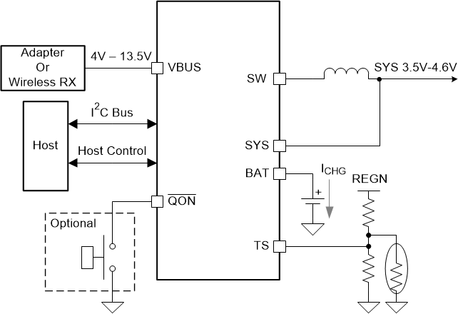
BQ25618E BQ25619E Simplified
                                                  Application Simplified Application