JAJSKU9B December   2022  – February 2024 BQ25628 , BQ25629

PRODUCTION DATA  

  1.   1
  2. 特長
  3. アプリケーション
  4. 概要
  5. 概要 (続き)
  6. Device Comparison
  7. Pin Configuration and Functions
  8. Specifications
    1. 7.1 Absolute Maximum Ratings
    2. 7.2 ESD Ratings
    3. 7.3 Recommended Operating Conditions
    4. 7.4 Thermal Information
    5. 7.5 Electrical Characteristics
    6. 7.6 Timing Requirements
    7. 7.7 Typical Characteristics
  9. Detailed Description
    1. 8.1 Overview
    2. 8.2 Functional Block Diagram
    3. 8.3 Feature Description
      1. 8.3.1  Power-On-Reset (POR)
      2. 8.3.2  Device Power Up from Battery
      3. 8.3.3  Device Power Up from Input Source
        1. 8.3.3.1 REGN LDO Power Up
        2. 8.3.3.2 Poor Source Qualification
        3. 8.3.3.3 D+/D– Detection Sets Input Current Limit (BQ25629)
        4. 8.3.3.4 ILIM Pin (BQ25628 Only)
        5. 8.3.3.5 Input Voltage Limit Threshold Setting (VINDPM Threshold)
        6. 8.3.3.6 Converter Power-Up
      4. 8.3.4  Power Path Management
        1. 8.3.4.1 Narrow VDC Architecture
        2. 8.3.4.2 Dynamic Power Management
        3. 8.3.4.3 High Impedance Mode
      5. 8.3.5  Battery Charging Management
        1. 8.3.5.1 Autonomous Charging Cycle
        2. 8.3.5.2 Battery Charging Profile
        3. 8.3.5.3 Charging Termination
        4. 8.3.5.4 Thermistor Qualification
          1. 8.3.5.4.1 Advanced Temperature Profile in Charge Mode
          2. 8.3.5.4.2 TS Pin Thermistor Configuration
          3. 8.3.5.4.3 Cold/Hot Temperature Window in OTG Mode
          4. 8.3.5.4.4 JEITA Charge Rate Scaling
          5. 8.3.5.4.5 TS_BIAS Pin
        5. 8.3.5.5 Charging Safety Timers
      6. 8.3.6  USB On-The-Go (OTG)
        1. 8.3.6.1 Boost OTG Mode
        2. 8.3.6.2 Bypass OTG Mode
        3. 8.3.6.3 PMID Voltage Indicator (PMID_GD)
      7. 8.3.7  Integrated 12-Bit ADC for Monitoring
      8. 8.3.8  Status Outputs ( STAT, INT)
        1. 8.3.8.1 Interrupts and Status, Flag and Mask Bits
        2. 8.3.8.2 Charging Status Indicator (STAT)
        3. 8.3.8.3 Interrupt to Host ( INT)
      9. 8.3.9  BATFET Control
        1. 8.3.9.1 Shutdown Mode
        2. 8.3.9.2 Ship Mode
        3. 8.3.9.3 System Power Reset
      10. 8.3.10 Protections
        1. 8.3.10.1 Voltage and Current Monitoring in Battery Only and HIZ Modes
          1. 8.3.10.1.1 Battery Undervoltage Lockout
          2. 8.3.10.1.2 Battery Overcurrent Protection
        2. 8.3.10.2 Voltage and Current Monitoring in Buck Mode
          1. 8.3.10.2.1 Input Overvoltage
          2. 8.3.10.2.2 System Overvoltage Protection (SYSOVP)
          3. 8.3.10.2.3 Forward Converter Cycle-by-Cycle Current Limit
          4. 8.3.10.2.4 System Short
          5. 8.3.10.2.5 Battery Overvoltage Protection (BATOVP)
          6. 8.3.10.2.6 Sleep and Poor Source Comparators
          7. 8.3.10.2.7 PMID OVP and VBUS Overcurrent
        3. 8.3.10.3 Voltage and Current Monitoring in Boost Mode
          1. 8.3.10.3.1 Boost Mode Overvoltage Protection
          2. 8.3.10.3.2 Boost Mode Duty Cycle Protection
          3. 8.3.10.3.3 Boost Mode PMID Undervoltage Protection
          4. 8.3.10.3.4 Boost Mode Battery Undervoltage
          5. 8.3.10.3.5 Boost Converter Cycle-by-Cycle Current Limit
          6. 8.3.10.3.6 Boost Mode SYS Short
        4. 8.3.10.4 Voltage and Current Monitoring in Bypass Mode
          1. 8.3.10.4.1 Bypass Mode Overvoltage Protection
          2. 8.3.10.4.2 Bypass Mode Battery OCP
          3. 8.3.10.4.3 Bypass Mode Reverse-Current Protection
          4. 8.3.10.4.4 Bypass Mode Battery Undervoltage
          5. 8.3.10.4.5 Bypass Mode SYS Short
          6. 8.3.10.4.6 Bypass Mode REGN Fault
        5. 8.3.10.5 Thermal Regulation and Thermal Shutdown
          1. 8.3.10.5.1 Thermal Protection in Buck Mode
          2. 8.3.10.5.2 Thermal Protection in Boost Mode
          3. 8.3.10.5.3 Thermal Protection in Battery-Only Mode
    4. 8.4 Device Functional Modes
      1. 8.4.1 Host Mode and Default Mode
      2. 8.4.2 Register Bit Reset
    5. 8.5 Programming
      1. 8.5.1 Serial Interface
        1. 8.5.1.1 Data Validity
        2. 8.5.1.2 START and STOP Conditions
        3. 8.5.1.3 Byte Format
        4. 8.5.1.4 Acknowledge (ACK) and Not Acknowledge (NACK)
        5. 8.5.1.5 Target Address and Data Direction Bit
        6. 8.5.1.6 Single Write and Read
        7. 8.5.1.7 Multi-Write and Multi-Read
    6. 8.6 Register Maps
      1. 8.6.1 Register Programming
      2. 8.6.2 BQ25628 Registers
  10. Application and Implementation
    1. 9.1 Application Information
    2. 9.2 Typical Application
      1. 9.2.1 Design Requirements
      2. 9.2.2 Detailed Design Procedure
        1. 9.2.2.1 Inductor Selection
        2. 9.2.2.2 Input Capacitor
        3. 9.2.2.3 Output Capacitor
      3. 9.2.3 Application Curves
  11. 10Power Supply Recommendations
  12. 11Layout
    1. 11.1 Layout Guidelines
    2. 11.2 Layout Example
  13. 12Device and Documentation Support
    1. 12.1 Device Support
      1. 12.1.1 サード・パーティ製品に関する免責事項
    2. 12.2 Documentation Support
      1. 12.2.1 Related Documentation
    3. 12.3 ドキュメントの更新通知を受け取る方法
    4. 12.4 サポート・リソース
    5. 12.5 Trademarks
    6. 12.6 静電気放電に関する注意事項
    7. 12.7 用語集
  14. 13Revision History
  15. 14Mechanical, Packaging, and Orderable Information

パッケージ・オプション

メカニカル・データ(パッケージ|ピン)
サーマルパッド・メカニカル・データ
発注情報

Application Curves

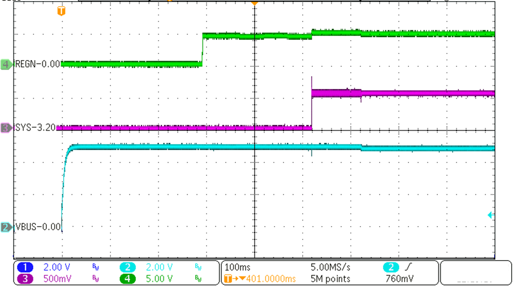
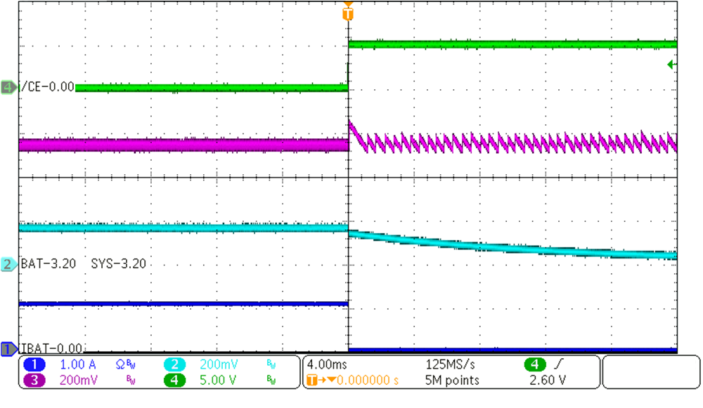
GUID-20230811-SS0I-BVDP-VGBF-PZRLZ2JZHCTS-low.png
VVBUS = 5 V VBAT = 3.2 V
ICHG = 1 A
Figure 9-3 Power-Up with Charge Enabled
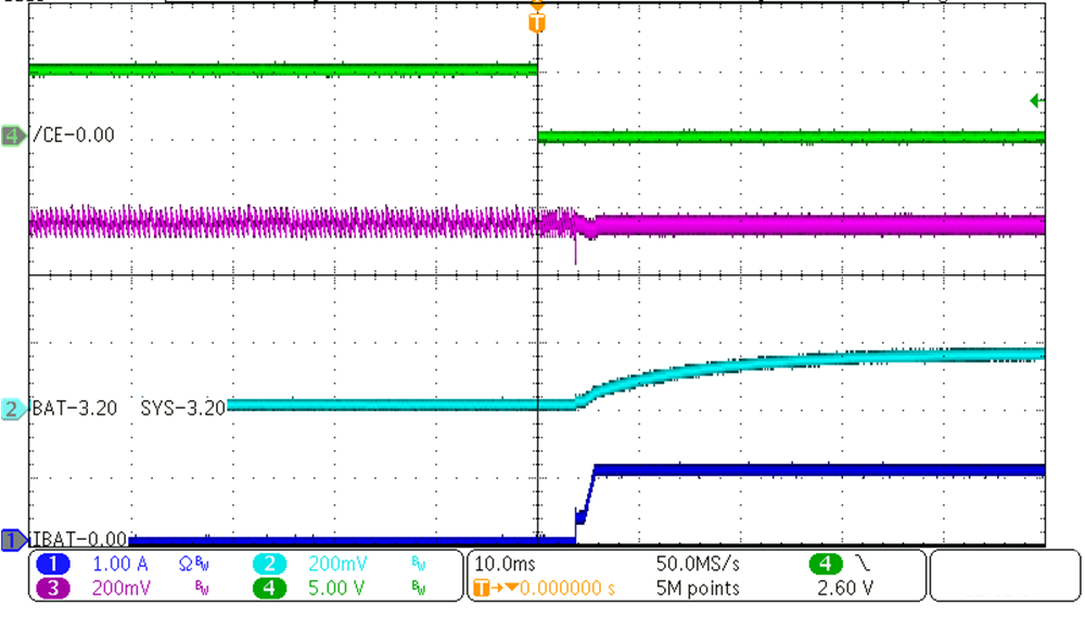
GUID-20220906-SS0I-QFW1-L1DQ-HRWBHX9GC0Q1-low.png
VVBUS = 5 V VBAT = 3.2 V
ICHG = 1 A
Figure 9-5 Charge Enable
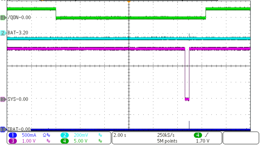
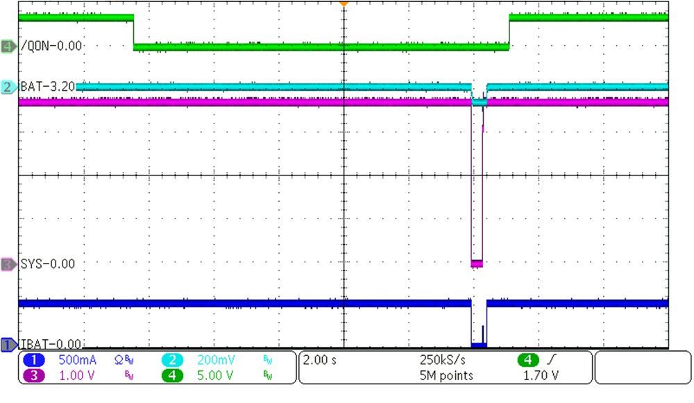
GUID-20220906-SS0I-GW4X-R1NL-TKQ7CWX4JN9M-low.png
VBAT = 3.2 V
Figure 9-7 System Reset by QON without VBUS Present
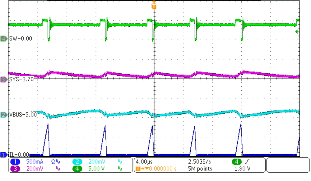
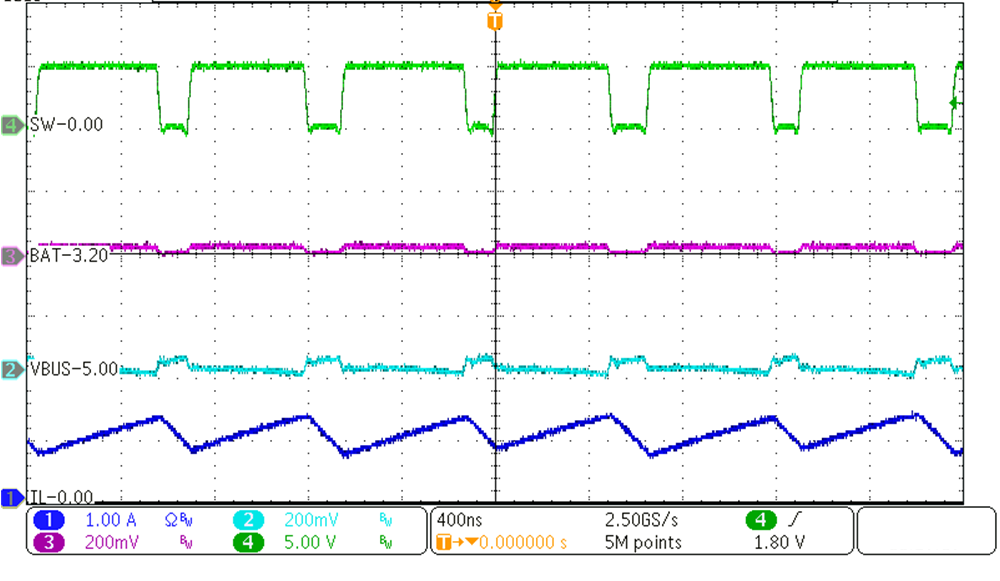
GUID-20220906-SS0I-RDFC-LD50-LHRZXLSNTR4M-low.png
VVBUS = 5 V VBAT = 3.2 V
ISYS = 50 mA Charge Disabled
Figure 9-9 PFM Switching in Buck Mode
GUID-20230412-SS0I-7RM8-BLS5-SDMPZRJCVGKT-low.png
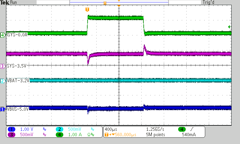
VVBUS = 5 V VBAT = 3.2 V
ISYS from 0 A to 1 A Charge Disabled
Figure 9-11 System Load Transient
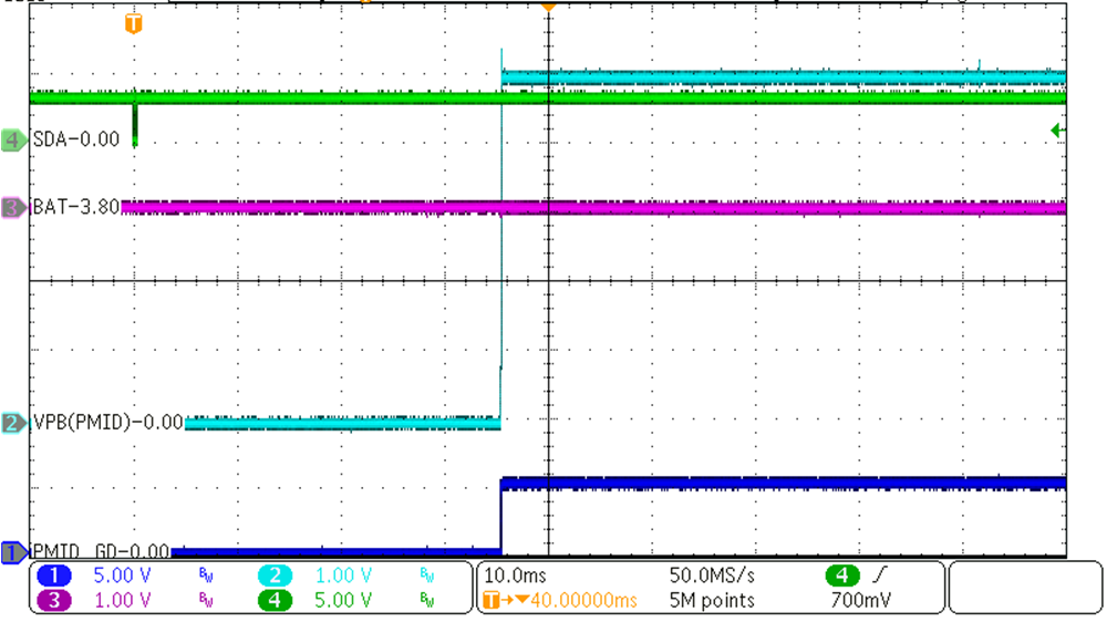
GUID-20221020-SS0I-ZWVM-RWRS-48VBB11XRVHD-low.png
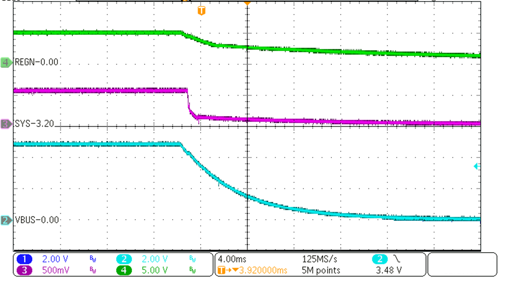
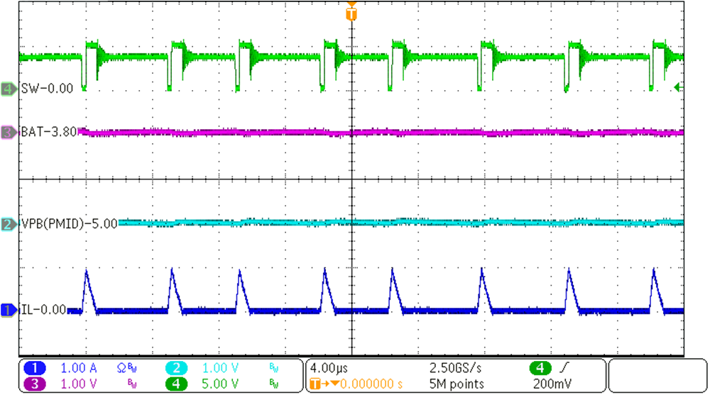
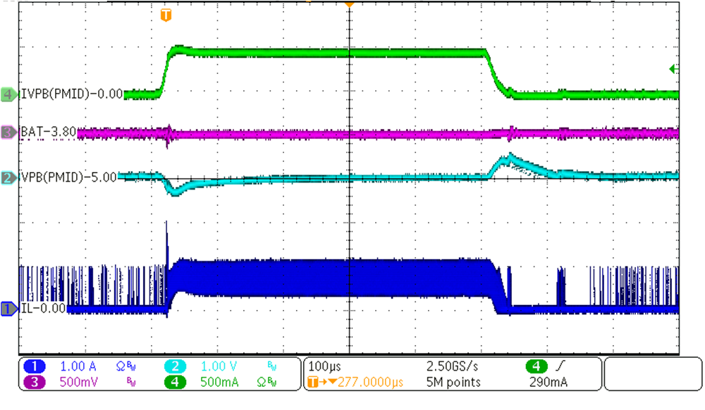
VBAT = 3.8 V VBOOST = 5.04V
IBOOST = 100 mA
Figure 9-13 Boost Mode Power Down
GUID-20221020-SS0I-XZNV-TDCT-LDHL6JN5CDSG-low.png
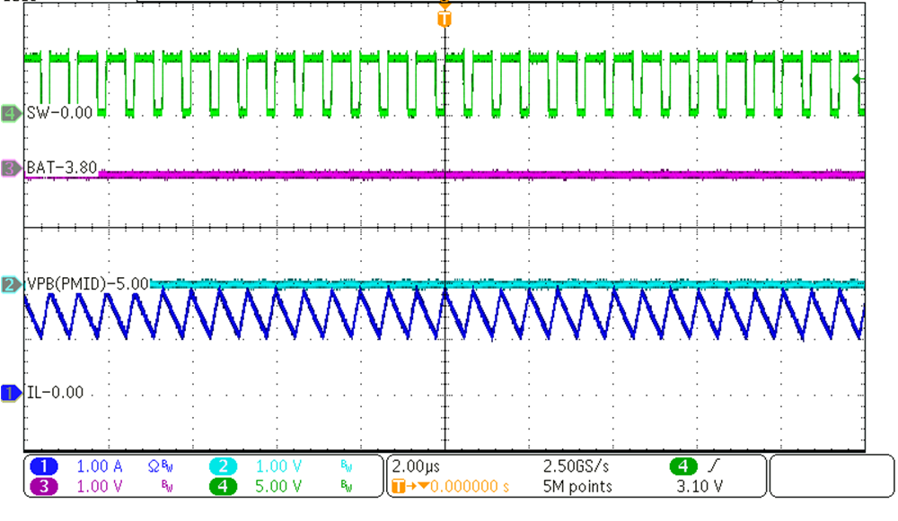
VBAT = 3.8 V VBOOST = 5.04V
IBOOST= 1 A
Figure 9-15 PWM Switching in Boost Mode
GUID-20230811-SS0I-BQDF-5JNG-JHCHK62MCD2J-low.png
VVBUS = 5 V VBAT = 3.2 V
ICHG = 1 A
Figure 9-4 Power-Down
GUID-20220906-SS0I-FNNV-SMNZ-X7LHBGRRVJMC-low.png
VVBUS = 5 V VBAT = 3.2 V
ICHG = 1 A
Figure 9-6 Charge Disable
GUID-20220906-SS0I-SQNN-7L69-R21VQGC6M1XP-low.png
VVBUS = 5 V VBAT = 3.2 V
ICHG = 480mA
Figure 9-8 System Reset by QON with VBUS Present
GUID-20220906-SS0I-M30T-8XM7-RTSC3WF2ZW2Z-low.png
VVBUS = 5 V VVBAT = 3.2 V
ICHG = 1 A
Figure 9-10 PWM Switching in Buck Mode
GUID-20221020-SS0I-1BBB-KWRW-FMVM6VKPF0LB-low.png
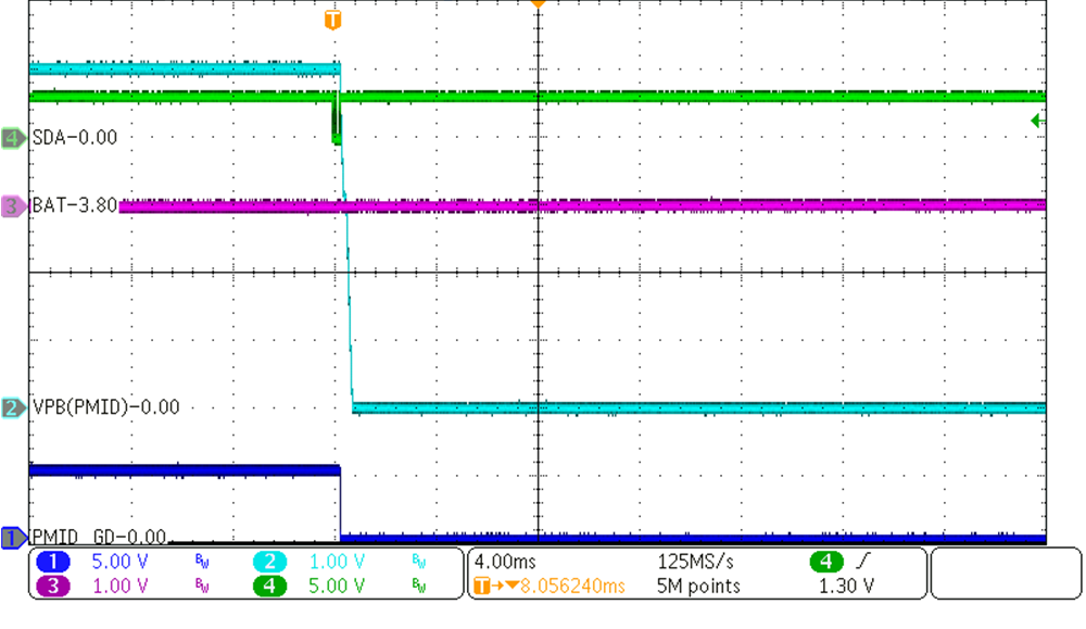
VBAT = 3.8 V VBOOST = 5.04 V
IBOOST = 100 mA
Figure 9-12 Boost Mode Power Up
GUID-20221020-SS0I-6KRD-MMDJ-HHB7CDC8RT3D-low.png
VBAT = 3.8 V VBOOST = 5.04V
IBOOST= 50 mA
Figure 9-14 PFM Switching in Boost Mode
GUID-20221020-SS0I-T8S2-19C1-RMMZGZQDRCG5-low.png
VBAT = 3.8 V VBOOST = 5.04 V
IBOOST from 5 mA to 500 mA
Figure 9-16 Boost Mode Load Transient